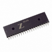
Z85C3010PSG Zilog, Z85C3010PSG Datasheet - Page 270

Z85C3010PSG
Manufacturer Part Number
Z85C3010PSG
Description
IC 10MHZ Z8500 CMOS SCC 40-DIP
Manufacturer
Zilog
Series
SCCr
Specifications of Z85C3010PSG
Processor Type
Z80
Features
Error Detection and Multiprotocol Support
Speed
10MHz
Voltage
5V
Mounting Type
Through Hole
Package / Case
40-DIP (0.620", 15.75mm)
Cpu Speed
8MHz
Digital Ic Case Style
DIP
No. Of Pins
40
Supply Voltage Range
5V
Operating Temperature Range
0°C To +70°C
Svhc
No SVHC (18-Jun-2010)
Base Number
85
Rohs Compliant
Yes
Clock Frequency
10MHz
Lead Free Status / RoHS Status
Lead free / RoHS Compliant
Other names
269-3934
Z85C3010PSG
Z85C3010PSG
Available stocks
Company
Part Number
Manufacturer
Quantity
Price
Company:
Part Number:
Z85C3010PSG
Manufacturer:
Zilog
Quantity:
135
Company:
Part Number:
Z85C3010PSG
Manufacturer:
Zilog
Quantity:
326
- Current page: 270 of 317
- Download datasheet (4Mb)
UM010901-0601
Listing 1 (Reference Appendix A for Listings 1 through 4)
shows the assembler code for this SCC initialization. Note
that the SCC is treated as a peripheral by the Z80181’s
MPU. For example, an I/O write to the scc_cont (address
e8H) or to the scc_data (address e9H) is a write to the
SCC’s control and data registers, respectively. As shown
in Listing 1, the SCC is initialized by issuing I/O writes to
the pointer and then to the control registers in an
alternating fashion. It is therefore very important that all
interrupts are disabled during this initialization routine.
The SCC is initially reset through software before
proceeding to program the other write registers. A NOP is
sufficient to provide the four PCLKs required by the SCC
recovery time after a soft reset. The SCC is programmed
for SDLC mode. The receive, transmit and external
interrupts are all initially disabled during this initialization.
Each of these interrupt sources are enabled at their proper
times in the main program. The SCC is programmed to
include status information in the vector that it places on the
bus in response to an interrupt acknowledge cycle (see
Listing 4 of the SCC interrupt vector table for all the
possible sources).
7.37 MHz
1/2
Technical Considerations When Implementing LocalTalk Link Access Protocol
= 16x230.4 kHz
3.6864 MHz
/RTxC
Figure 3. SCC Clocking Scheme
/TRxC
/RTxC
Since SDLC is bit-oriented, the transmitter and receiver
are both programmed for 8 bits per character as required
by LLAP. Address filtering is implemented by setting the
Address Search Mode bit 2 on WR3. Setting this bit
causes messages with addresses not matching the
address programmed in WR6 and not matching the
broadcast address to be rejected. Values in WR10 presets
the CRCs to ones, sets the encoding to FM0 mode and
makes certain that transmission of flags occur during idle
and underrun conditions. WR11 is set so that the receive
clock is sourced by the DPLL output; the transmit clock is
sourced by the Baud Rate Generator output; /TRxC’s
output is from the BRG. The input to the BRG is from the
/RTxC.
The BRG’s time constant is loaded in WR13 and WR12 so
that the /RTxC’s 3.6864 MHz signal is divided by 16 in
order to obtain a 230.4 kHz signal for the transmitter clock.
WR14 makes certain that the DPLL is disabled before
choosing the clock source and operating mode. The DPLL
is enabled by issuing the Enter Search Mode in WR14.
DPLL
DPLL
BRG
/16
RxDPLL Out
BRG Out
230.4 kHz
Rx
Rx
Tx
Tx
Receiver
Transmitter
Application Note
6-135
1
Related parts for Z85C3010PSG
Image
Part Number
Description
Manufacturer
Datasheet
Request
R

Part Number:
Description:
Manufacturer:
Zilog, Inc.
Datasheet:

Part Number:
Description:
Cmos Scc Serial Communications Controller
Manufacturer:
ZiLOG Semiconductor
Datasheet:

Part Number:
Description:
Communication Controllers, ZILOG INTELLIGENT PERIPHERAL CONTROLLER (ZIP)
Manufacturer:
Zilog, Inc.
Datasheet:

Part Number:
Description:
KIT DEV FOR Z8 ENCORE 16K TO 64K
Manufacturer:
Zilog
Datasheet:

Part Number:
Description:
KIT DEV Z8 ENCORE XP 28-PIN
Manufacturer:
Zilog
Datasheet:

Part Number:
Description:
DEV KIT FOR Z8 ENCORE 8K/4K
Manufacturer:
Zilog
Datasheet:

Part Number:
Description:
KIT DEV Z8 ENCORE XP 28-PIN
Manufacturer:
Zilog
Datasheet:

Part Number:
Description:
DEV KIT FOR Z8 ENCORE 4K TO 8K
Manufacturer:
Zilog
Datasheet:

Part Number:
Description:
CMOS Z8 microcontroller. ROM 16 Kbytes, RAM 256 bytes, speed 16 MHz, 32 lines I/O, 3.0V to 5.5V
Manufacturer:
Zilog, Inc.
Datasheet:

Part Number:
Description:
Low-cost microcontroller. 512 bytes ROM, 61 bytes RAM, 8 MHz
Manufacturer:
Zilog, Inc.
Datasheet:

Part Number:
Description:
Z8 4K OTP Microcontroller
Manufacturer:
Zilog, Inc.
Datasheet:

Part Number:
Description:
CMOS SUPER8 ROMLESS MCU
Manufacturer:
Zilog, Inc.
Datasheet:

Part Number:
Description:
SL1866 CMOSZ8 OTP Microcontroller
Manufacturer:
Zilog, Inc.
Datasheet:


