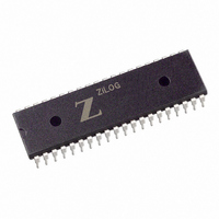
Z85C3010PSG Zilog, Z85C3010PSG Datasheet - Page 218

Z85C3010PSG
Manufacturer Part Number
Z85C3010PSG
Description
IC 10MHZ Z8500 CMOS SCC 40-DIP
Manufacturer
Zilog
Series
SCCr
Specifications of Z85C3010PSG
Processor Type
Z80
Features
Error Detection and Multiprotocol Support
Speed
10MHz
Voltage
5V
Mounting Type
Through Hole
Package / Case
40-DIP (0.620", 15.75mm)
Cpu Speed
8MHz
Digital Ic Case Style
DIP
No. Of Pins
40
Supply Voltage Range
5V
Operating Temperature Range
0°C To +70°C
Svhc
No SVHC (18-Jun-2010)
Base Number
85
Rohs Compliant
Yes
Clock Frequency
10MHz
Lead Free Status / RoHS Status
Lead free / RoHS Compliant
Other names
269-3934
Z85C3010PSG
Z85C3010PSG
Available stocks
Company
Part Number
Manufacturer
Quantity
Price
Company:
Part Number:
Z85C3010PSG
Manufacturer:
Zilog
Quantity:
135
Company:
Part Number:
Z85C3010PSG
Manufacturer:
Zilog
Quantity:
326
- Current page: 218 of 317
- Download datasheet (4Mb)
UM010901-0601
When the Z8002 CPU uses the lower half of the
Address/Data bus (AD0-AD7 the least significant byte) for
byte read and write transactions during I/O operations,
these transactions are performed between the CPU and
I/O ports located at odd I/O addresses. Since the Z-SCC is
attached to the CPU on the lower half of the A/D bus, its
registers must appear to the CPU at odd I/O addresses. To
achieve this, the Z-SCC can be programmed to select its
internal registers using lines AD5-AD1. This is done either
automatically with the Force Hardware Reset command in
WR9 or by sending a Select Shift Left Mode command to
INITIALIZATION
The Z-SCC can be initialized for use in different modes by
setting various bits in its Write registers. First, a hardware
reset must be performed by setting bits 7 and 6 of WR9 to
one; the rest of the bits are disabled by writing a logic zero.
Bisync mode is established by selecting a 16-bit sync
character, Sync Mode Enable, and a Xl clock in WR4. A
data rate of 9600 baud, NRZ encoding, and a data
character length of eight bits are among the other options
that are selected in this example (Table 2).
Note that WR9 is accessed twice, first to perform a
hardware reset and again at the end of the initialization
sequence to enable the interrupts. The programming
sequence depicted in Table 2 establishes the necessary
parameters for the receiver and the transmitter so that,
when enabled, they are ready to perform communication
tasks. To avoid internal race and false interrupt conditions,
it is important to initialize the registers in the sequence
depicted in this application note.
WR0B in channel B of the Z-SCC. For this application, the
Z-SCC registers are located at I/O port address ‘FExx’.
The Chip Select signal (/CS0) is derived by decoding I/O
address ‘FE’ hex from lines AD15-AD8 of the controller.
The Read/Write registers are automatically selected by the
Z-SCC when internally decoding lines AD5-AD1 in Shift
Left
automatically, the Z-SCC decodes lines AD5-AD1 in Shift
Left mode. The register map for the Z-SCC is depicted in
Table 1.
Address
(hex)
FE01
FE03
FE05
FE07
FE09
FE0B
FE0D
FE0F
FE11
FE13
FE15
FE17
FE19
FE1B
FE1D
FE1F
FE21
FE23
FE25
FE27
FE29
FE2B
FE2D
FE2F
FE31
FE33
FE35
FE37
FE39
FE3B
FE3D
FE3F
mode.
SCC in Binary Synchronous Communications
To
Table 1. Register Map
select
Write Register
WR10B
WR11B
WR12B
WR13B
WR14B
WR15B
WR10A
WR11A
WR12A
WR13A
WR14A
WR15A
B DATA
A DATA
WR0B
WR1B
WR3B
WR4B
WR5B
WR6B
WR7B
WR0A
WR1A
WR3A
WR4A
WR5A
WR6A
WR7A
WR2
WR9
WR2
WR9
the
Read/Write
Application Note
Read Register
B DATA
RR10B
RR12B
RR13B
RR15B
A DATA
RR10A
RR12A
RR13A
RR15A
RR0B
RR1B
RR2B
RR3B
RR0A
RR1A
RR2A
RR3A
registers
6-83
9
Related parts for Z85C3010PSG
Image
Part Number
Description
Manufacturer
Datasheet
Request
R

Part Number:
Description:
Manufacturer:
Zilog, Inc.
Datasheet:

Part Number:
Description:
Cmos Scc Serial Communications Controller
Manufacturer:
ZiLOG Semiconductor
Datasheet:

Part Number:
Description:
Communication Controllers, ZILOG INTELLIGENT PERIPHERAL CONTROLLER (ZIP)
Manufacturer:
Zilog, Inc.
Datasheet:

Part Number:
Description:
KIT DEV FOR Z8 ENCORE 16K TO 64K
Manufacturer:
Zilog
Datasheet:

Part Number:
Description:
KIT DEV Z8 ENCORE XP 28-PIN
Manufacturer:
Zilog
Datasheet:

Part Number:
Description:
DEV KIT FOR Z8 ENCORE 8K/4K
Manufacturer:
Zilog
Datasheet:

Part Number:
Description:
KIT DEV Z8 ENCORE XP 28-PIN
Manufacturer:
Zilog
Datasheet:

Part Number:
Description:
DEV KIT FOR Z8 ENCORE 4K TO 8K
Manufacturer:
Zilog
Datasheet:

Part Number:
Description:
CMOS Z8 microcontroller. ROM 16 Kbytes, RAM 256 bytes, speed 16 MHz, 32 lines I/O, 3.0V to 5.5V
Manufacturer:
Zilog, Inc.
Datasheet:

Part Number:
Description:
Low-cost microcontroller. 512 bytes ROM, 61 bytes RAM, 8 MHz
Manufacturer:
Zilog, Inc.
Datasheet:

Part Number:
Description:
Z8 4K OTP Microcontroller
Manufacturer:
Zilog, Inc.
Datasheet:

Part Number:
Description:
CMOS SUPER8 ROMLESS MCU
Manufacturer:
Zilog, Inc.
Datasheet:

Part Number:
Description:
SL1866 CMOSZ8 OTP Microcontroller
Manufacturer:
Zilog, Inc.
Datasheet:


