R0K561622S000BE Renesas Electronics America, R0K561622S000BE Datasheet - Page 908
R0K561622S000BE
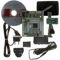
Manufacturer Part Number
R0K561622S000BE
Description
KIT STARTER FOR H8SX/1622
Manufacturer
Renesas Electronics America
Series
Renesas Starter Kits (RSK)r
Type
MCUr
Specifications of R0K561622S000BE
Contents
Board, Cables, CD, Debugger, Power Supply
Silicon Manufacturer
Renesas
Features
Coding And Debugging, E10A Emulator, RS232 Serial Connection
Kit Contents
Board
Silicon Family Name
H8SX/1622F
Silicon Core Number
R5F61622N50LGV
Lead Free Status / RoHS Status
Lead free / RoHS Compliant
For Use With/related Products
H8SX/1622
Lead Free Status / RoHS Status
Lead free / RoHS Compliant, Lead free / RoHS Compliant


Section 23 Clock Pulse Generator
23.5
23.5.1
1. The following points should be noted since the frequency of φ (Iφ: system clock, Pφ:
2. All the on-chip peripheral modules (except for the DMAC and DTC) operate on the Pφ.
3. The relationship among the system clock, peripheral module clock, and external bus clock is Iφ
4. Figure 23.6 shows the clock modification timing. After a value is written to SCKCR, this LSI
Rev. 2.00 Sep. 16, 2009 Page 878 of 1036
REJ09B0414-0200
peripheral module clock, Bφ: external bus clock) supplied to each module changes according
to the setting of SCKCR.
Select a clock division ratio that is within the operation guaranteed range of clock cycle time
t
The setting should be within the operation guaranteed range of 8 MHz ≤ Iφ ≤ 50 MHz, 8 MHz
≤ Pφ ≤ 35 MHz, and 8 MHz ≤ Bφ ≤ 50 MHz.
Therefore, note that the time processing of modules such as a timer and SCI differs before and
after changing the clock division ratio.
In addition, wait time for clearing software standby mode differs by changing the clock
division ratio. For details, see section 24.7.3, Setting Oscillation Settling Time after Exit from
Software Standby Mode.
≥ Pφ and Iφ ≥ Bφ. In addition, the system clock setting has the highest priority. Accordingly,
Pφ or Bφ may have the frequency set by bits ICK2 to ICK0 regardless of the settings of bits
PCK2 to PCK0 or BCK2 to BCK0.
waits for the current bus cycle to complete. After the current bus cycle completes, each clock
frequency will be modified within one cycle (worst case) of the external input clock φ.
cyc
shown in the AC timing of electrical characteristics.
Usage Notes
Notes on Clock Pulse Generator
Related parts for R0K561622S000BE
Image
Part Number
Description
Manufacturer
Datasheet
Request
R

Part Number:
Description:
KIT STARTER FOR M16C/29
Manufacturer:
Renesas Electronics America
Datasheet:

Part Number:
Description:
KIT STARTER FOR R8C/2D
Manufacturer:
Renesas Electronics America
Datasheet:

Part Number:
Description:
R0K33062P STARTER KIT
Manufacturer:
Renesas Electronics America
Datasheet:

Part Number:
Description:
KIT STARTER FOR R8C/23 E8A
Manufacturer:
Renesas Electronics America
Datasheet:

Part Number:
Description:
KIT STARTER FOR R8C/25
Manufacturer:
Renesas Electronics America
Datasheet:

Part Number:
Description:
KIT STARTER H8S2456 SHARPE DSPLY
Manufacturer:
Renesas Electronics America
Datasheet:

Part Number:
Description:
KIT STARTER FOR R8C38C
Manufacturer:
Renesas Electronics America
Datasheet:

Part Number:
Description:
KIT STARTER FOR R8C35C
Manufacturer:
Renesas Electronics America
Datasheet:

Part Number:
Description:
KIT STARTER FOR R8CL3AC+LCD APPS
Manufacturer:
Renesas Electronics America
Datasheet:
Part Number:
Description:
KIT STARTER FOR RX610
Manufacturer:
Renesas Electronics America
Datasheet:

Part Number:
Description:
KIT STARTER FOR R32C/118
Manufacturer:
Renesas Electronics America
Datasheet:

Part Number:
Description:
KIT DEV RSK-R8C/26-29
Manufacturer:
Renesas Electronics America
Datasheet:

Part Number:
Description:
KIT STARTER FOR SH7124
Manufacturer:
Renesas Electronics America
Datasheet:

Part Number:
Description:
KIT DEV FOR SH7203
Manufacturer:
Renesas Electronics America
Datasheet:
Part Number:
Description:
KIT STARTER FOR R8C/18191A1B
Manufacturer:
Renesas Electronics America
Datasheet: