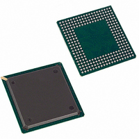
DS31256 Maxim Integrated Products, DS31256 Datasheet - Page 138

DS31256
Manufacturer Part Number
DS31256
Description
IC CTRLR HDLC 256-CHANNEL 256BGA
Manufacturer
Maxim Integrated Products
Datasheet
1.DS31256.pdf
(183 pages)
Specifications of DS31256
Controller Type
HDLC Controller
Interface
Serial
Voltage - Supply
3 V ~ 3.6 V
Current - Supply
500mA
Operating Temperature
0°C ~ 70°C
Mounting Type
Surface Mount
Package / Case
256-BGA
Lead Free Status / RoHS Status
Contains lead / RoHS non-compliant
Available stocks
Company
Part Number
Manufacturer
Quantity
Price
Part Number:
DS31256
Manufacturer:
DALLAS
Quantity:
20 000
10.2.1
Bit 0/I/O Space Control (IOC). This read-only bit is forced to 0 by the device to indicate that it does not respond
to I/O space accesses.
Bit 1/Memory Space Control (MSC). This read/write bit controls whether or not the device responds to accesses
by the PCI bus to the memory space (the internal device configuration registers). When this bit is set to 0, the
device ignores accesses attempted to the internal configuration registers. When set to 1, the device allows accesses
to the internal configuration registers. This bit should be set to 0 when the local bus is operated in the
configuration mode. This bit is forced to 0 when a hardware reset is initiated through the PRST pin.
Bit 2/Master Control (MASC). This read/write bit controls whether or not the device can act as a master on the
PCI bus. When this bit is set to 0, the device cannot act as a master. When it is set to 1, the device can act as a bus
master. This bit is forced to 0 when a hardware reset is initiated through the PRST pin.
Bit 3/Special Cycle Control (SCC). This read-only bit is forced to 0 by the device to indicate that it cannot
decode special cycle operations.
Bit 4/Memory Write and Invalidate Command Enable (MWEN). This read-only bit is forced to 0 by the
device to indicate that it cannot generate the memory write and invalidate command.
Bit 5/VGA Control (VGA). This read-only bit is forced to 0 by the device to indicate that it is not a VGA-
compatible device.
Bit 6/Parity Error Response Control (PARC). This read/write bit controls whether or not the device should
ignore parity errors. When this bit is set to 0, the device ignores any parity errors that it detects and continues to
operate normally. When this bit is set to 1, the device must act on parity errors. This bit is forced to 0 when a
hardware reset is initiated through the PRST pin.
Bit 7/Address Stepping Control (STEPC). This read-only bit is forced to 0 by the device to indicate that it is not
capable of address/data stepping.
Bit 8/PCI System Error Control (PSEC). This read/write bit controls whether or not the device should enable
the PSERR output pin. When this bit is set to 0, the device disables the PSERR pin. When this bit is set to 1, the
device enables the PSERR pin. This bit is forced to 0 when a hardware reset is initiated through the PRST pin.
Bit 9/Fast Back-to-Back Master Enable (FBBEN). This read-only bit is forced to 0 by the device to indicate that
it is not capable of generating fast back-to-back transactions to different agents.
Bits 10 to 15/Reserved. These read-only bits are forced to 0 by the device.
0 = ignore accesses to the internal device configuration registers
1 = allow accesses to the internal device configuration registers
0 = deny the device from operating as a bus master
1 = allow the device to operate as a bus master
0 = ignore parity errors
1 = act on parity errors
0 = disable the PSERR pin
1 = enable the PSERR pin
Command Bits (PCMD0)
138 of 183


