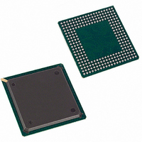
DS31256 Maxim Integrated Products, DS31256 Datasheet - Page 141

DS31256
Manufacturer Part Number
DS31256
Description
IC CTRLR HDLC 256-CHANNEL 256BGA
Manufacturer
Maxim Integrated Products
Datasheet
1.DS31256.pdf
(183 pages)
Specifications of DS31256
Controller Type
HDLC Controller
Interface
Serial
Voltage - Supply
3 V ~ 3.6 V
Current - Supply
500mA
Operating Temperature
0°C ~ 70°C
Mounting Type
Surface Mount
Package / Case
256-BGA
Lead Free Status / RoHS Status
Contains lead / RoHS non-compliant
Available stocks
Company
Part Number
Manufacturer
Quantity
Price
Part Number:
DS31256
Manufacturer:
DALLAS
Quantity:
20 000
Register Name:
Register Description:
Register Address:
MSB
Note: Read-only bits in the PDCM register are underlined; all other bits are read-write.
Bit 0/Memory Space Indicator (MSI). This read-only bit is forced to 0 to indicate that the internal device
configuration registers are mapped to memory space.
Bits 1, 2/Type 0, Type 1. These read-only bits are forced to 00b to indicate that the internal device configuration
registers can be mapped anywhere in the 32-bit address space.
Bit 3/Prefetchable (PF). This read-only bit is forced to 0 to indicate that prefetching is not supported by the
device for the internal device configuration registers.
Bits 4 to 11/Base Address. These read-only bits are forced to 0 to indicate that the internal device configuration
registers require 4kB of memory space.
Bits 12 to 31/Base Address. These read/write bits define the location of the 4kB memory space that is mapped to
the internal configuration registers. These bits correspond to the most significant bits of the PCI address space.
Register Name:
Register Description:
Register Address:
MSB
Bits 0 to 7/Interrupt Line. These read/write bits indicate and store interrupt line routing information. The device
does not use this information, it is only posted here for the host to use.
Bits 8 to 15/Interrupt Pin. These read-only bits are forced to 01h to indicate that PINTA is used as an interrupt.
Bits 16 to 23/Minimum Grant. These read-only bits are used to indicate to the host how long of a burst period
the device needs, assuming a clock rate of 33MHz. The values placed in these bits specify a period of time in
0.25µs increments. These bits are forced to 05h.
Bits 24 to 31/Maximum Latency. These read-only bits are used to indicate to the host how often the device needs
to gain access to the PCI bus. The values placed in these bits specify a period of time in 0.25µs increments. These
bits are forced to 0Fh.
Base Address (Read Only/Set to 0h)
Base Address
PDCM
PCI Device Configuration Memory Base Address Register
0x010h
PINTL0
PCI Interrupt Line and Pin/Minimum Grant/Maximum Latency Register 0
0x03Ch
Maximum Latency (Read Only/Set to 0 Fh)
Maximum Grant (Read Only/Set to 05h)
Interrupt Pin (Read Only/Set to 01h)
141 of 183
Interrupt Line
Base Address
Base Address
PF
Base Address (Read Only/Set to 0h)
TYPE1
TYPE0
LSB
MSI
LSB


