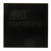
AT32AP7002-CTUT Atmel, AT32AP7002-CTUT Datasheet - Page 316

AT32AP7002-CTUT
Manufacturer Part Number
AT32AP7002-CTUT
Description
IC MCU 32BIT AVR32 196-CBGA
Manufacturer
Atmel
Series
AVR®32 AP7r
Specifications of AT32AP7002-CTUT
Core Processor
AVR
Core Size
32-Bit
Speed
150MHz
Connectivity
EBI/EMI, I²C, MMC, PS2, SPI, SSC, UART/USART, USB
Peripherals
AC'97, DMA, I²C, LCD, POR, PWM, WDT
Number Of I /o
85
Program Memory Type
ROMless
Ram Size
32K x 8
Voltage - Supply (vcc/vdd)
1.65 V ~ 1.95 V
Data Converters
D/A 2x16b
Oscillator Type
Internal
Operating Temperature
-40°C ~ 85°C
Package / Case
196-CBGA
Data Bus Width
32 bit
Data Ram Size
32 KB
Interface Type
I2C, JTAG, PS2, SPI, SSC, UART, USART, USB
Maximum Clock Frequency
150 MHz
Number Of Timers
3
Maximum Operating Temperature
+ 85 C
Mounting Style
SMD/SMT
Minimum Operating Temperature
- 40 C
On-chip Dac
16 bit, 2 Channel
Package
196CTBGA
Device Core
AVR32
Family Name
AT32
Maximum Speed
150 MHz
Operating Supply Voltage
1.8|3.3 V
For Use With
ATAVRONEKIT - KIT AVR/AVR32 DEBUGGER/PROGRMMRATNGW100 - KIT AVR32 NETWORK GATEWAYATSTK1000 - KIT STARTER FOR AVR32AP7000
Lead Free Status / RoHS Status
Lead free / RoHS Compliant
Eeprom Size
-
Program Memory Size
-
Lead Free Status / Rohs Status
Details
Available stocks
Company
Part Number
Manufacturer
Quantity
Price
- Current page: 316 of 896
- Download datasheet (13Mb)
21.6
21.6.1
21.6.2
21.6.3
32054F–AVR32–09/09
Functional Description
Transfer format
Modes of Operation
Transmitting Data
The data put on the TWD line must be 8 bits long. Data is transferred MSB first; each byte must
be followed by an acknowledgement. The number of bytes per transfer is unlimited (see
21-4 on page
Each transfer begins with a START condition and terminates with a STOP condition (see
21-3 on page
Figure 21-3.
Figure 21-4. Transfer Format
The TWI has two modes of operation:
The TWI Control Register (CR) allows configuration of the interface in Master Mode. In this
mode, it generates the clock according to the value programmed in the Clock Waveform Gener-
ator Register (CWGR). This register defines the TWCK signal completely, enabling the interface
to be adapted to a wide range of clocks.
After the master initiates a Start condition, it sends a 7-bit slave address, configured in the Mas-
ter Mode register (DADR in MMR), to notify the slave device. The bit following the slave address
indicates the transfer direction (write or read). If this bit is 0, it indicates a write operation (trans-
mit operation). If the bit is 1, it indicates a request for data read (receive operation).
The TWI transfers require the slave to acknowledge each received byte. During the acknowl-
edge clock pulse, the master releases the data line (HIGH), enabling the slave to pull it down in
order to generate the acknowledge. The master polls the data line during this clock pulse and
sets the NAK bit in the status register if the slave does not acknowledge the byte. As with the
•A high-to-low transition on the TWD line while TWCK is high defines the START condition.
•A low-to-high transition on the TWD line while TWCK is high defines a STOP condition.
•Master transmitter mode
•Master receiver mode
TWD
TWCK
316).
316).
START and STOP Conditions
Start
Address
TWCK
TWD
R/W
Start
Ack
Data
Ack
Data
Stop
AT32AP7002
Ack
Stop
Figure
Figure
316
Related parts for AT32AP7002-CTUT
Image
Part Number
Description
Manufacturer
Datasheet
Request
R

Part Number:
Description:
DEV KIT FOR AVR/AVR32
Manufacturer:
Atmel
Datasheet:

Part Number:
Description:
INTERVAL AND WIPE/WASH WIPER CONTROL IC WITH DELAY
Manufacturer:
ATMEL Corporation
Datasheet:

Part Number:
Description:
Low-Voltage Voice-Switched IC for Hands-Free Operation
Manufacturer:
ATMEL Corporation
Datasheet:

Part Number:
Description:
MONOLITHIC INTEGRATED FEATUREPHONE CIRCUIT
Manufacturer:
ATMEL Corporation
Datasheet:

Part Number:
Description:
AM-FM Receiver IC U4255BM-M
Manufacturer:
ATMEL Corporation
Datasheet:

Part Number:
Description:
Monolithic Integrated Feature Phone Circuit
Manufacturer:
ATMEL Corporation
Datasheet:

Part Number:
Description:
Multistandard Video-IF and Quasi Parallel Sound Processing
Manufacturer:
ATMEL Corporation
Datasheet:

Part Number:
Description:
High-performance EE PLD
Manufacturer:
ATMEL Corporation
Datasheet:

Part Number:
Description:
8-bit Flash Microcontroller
Manufacturer:
ATMEL Corporation
Datasheet:

Part Number:
Description:
2-Wire Serial EEPROM
Manufacturer:
ATMEL Corporation
Datasheet:


