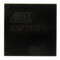
AT32AP7002-CTUT Atmel, AT32AP7002-CTUT Datasheet - Page 807

AT32AP7002-CTUT
Manufacturer Part Number
AT32AP7002-CTUT
Description
IC MCU 32BIT AVR32 196-CBGA
Manufacturer
Atmel
Series
AVR®32 AP7r
Specifications of AT32AP7002-CTUT
Core Processor
AVR
Core Size
32-Bit
Speed
150MHz
Connectivity
EBI/EMI, I²C, MMC, PS2, SPI, SSC, UART/USART, USB
Peripherals
AC'97, DMA, I²C, LCD, POR, PWM, WDT
Number Of I /o
85
Program Memory Type
ROMless
Ram Size
32K x 8
Voltage - Supply (vcc/vdd)
1.65 V ~ 1.95 V
Data Converters
D/A 2x16b
Oscillator Type
Internal
Operating Temperature
-40°C ~ 85°C
Package / Case
196-CBGA
Data Bus Width
32 bit
Data Ram Size
32 KB
Interface Type
I2C, JTAG, PS2, SPI, SSC, UART, USART, USB
Maximum Clock Frequency
150 MHz
Number Of Timers
3
Maximum Operating Temperature
+ 85 C
Mounting Style
SMD/SMT
Minimum Operating Temperature
- 40 C
On-chip Dac
16 bit, 2 Channel
Package
196CTBGA
Device Core
AVR32
Family Name
AT32
Maximum Speed
150 MHz
Operating Supply Voltage
1.8|3.3 V
For Use With
ATAVRONEKIT - KIT AVR/AVR32 DEBUGGER/PROGRMMRATNGW100 - KIT AVR32 NETWORK GATEWAYATSTK1000 - KIT STARTER FOR AVR32AP7000
Lead Free Status / RoHS Status
Lead free / RoHS Compliant
Eeprom Size
-
Program Memory Size
-
Lead Free Status / Rohs Status
Details
Available stocks
Company
Part Number
Manufacturer
Quantity
Price
- Current page: 807 of 896
- Download datasheet (13Mb)
35.4.2
35.4.3
35.5
35.5.1
32054F–AVR32–09/09
Functional Description
Power Management
Interrupt
Data Timing
The ISI clock is generated by the Power Manager. Before using the ISI, the programmer must
ensure that the ISIclock is enabled in the Power Manager.
In the ISI description, Master Clock (MCK) is the clock of the peripheral bus to which the ISI is
connected.
To prevent bus errors the ISI operation must be terminated before entering sleep mode
The ISI interface has an interrupt line connected to the Interrupt Controller. Handling the ISI
interrupt requires programming the interrupt controller before configuring the ISI.
The Image Sensor Interface (ISI) supports direct connection to the International Telecommuni-
cation Union Recommendation ITU-R BT. 601/656 8-bit mode compliant sensors and up to 12-
bit grayscale sensors. It receives the image data stream from the image sensor on the 12-bit
data bus.
This module receives up to 12 bits for data, the horizontal and vertical synchronizations and the
pixel clock. The reduced pin count alternative for synchronization is supported for sensors that
embed SAV (start of active video) and EAV (end of active video) delimiters in the data stream.
The Image Sensor Interface interrupt line is generally connected to the Interrupt Controller and
can trigger an interrupt at the beginning of each frame and at the end of a DMA frame transfer. If
the SAV/EAV synchronization is used, an interrupt can be triggered on each delimiter event.
For 8-bit color sensors, the data stream received can be in several possible formats: YCbCr
4:2:2, RGB 8:8:8, RGB 5:6:5 and may be processed before the storage in memory. The data
stream may be sent on both preview path and codec path if the bit CODEC_ON in the CR1 is
one. To optimize the bandwidth, the codec path should be enabled only when a capture is
required.
In grayscale mode, the input data stream is stored in memory without any processing. The 12-bit
data, which represent the grayscale level for the pixel, is stored in memory one or two pixels per
word, depending on the GS_MODE bit in the CR2 register. The codec datapath is not available
when grayscale image is selected.
A frame rate counter allows users to capture all frames or 1 out of every 2 to 8 frames.
The two data timings using horizontal and vertical synchronization and EAV/SAV sequence syn-
chronization are shown in
In the VSYNC/HSYNC synchronization, the valid data is captured with the active edge of the
pixel clock (PCK), after SFD lines of vertical blanking and SLD pixel clock periods delay pro-
grammed in the control register.
The ITU-RBT.656-4 defines the functional timing for an 8-bit wide interface.
There are two timing reference signals, one at the beginning of each video data block SAV
(0xFF000080) and one at the end of each video data block EAV(0xFF00009D). Only data sent
between EAV and SAV is captured. Horizontal blanking and vertical blanking are ignored. Use of
the SAV and EAV synchronization eliminates the VSYNC and HSYNC signals from the inter-
Figure 35-3
and
Figure
35-4.
AT32AP7002
807
Related parts for AT32AP7002-CTUT
Image
Part Number
Description
Manufacturer
Datasheet
Request
R

Part Number:
Description:
DEV KIT FOR AVR/AVR32
Manufacturer:
Atmel
Datasheet:

Part Number:
Description:
INTERVAL AND WIPE/WASH WIPER CONTROL IC WITH DELAY
Manufacturer:
ATMEL Corporation
Datasheet:

Part Number:
Description:
Low-Voltage Voice-Switched IC for Hands-Free Operation
Manufacturer:
ATMEL Corporation
Datasheet:

Part Number:
Description:
MONOLITHIC INTEGRATED FEATUREPHONE CIRCUIT
Manufacturer:
ATMEL Corporation
Datasheet:

Part Number:
Description:
AM-FM Receiver IC U4255BM-M
Manufacturer:
ATMEL Corporation
Datasheet:

Part Number:
Description:
Monolithic Integrated Feature Phone Circuit
Manufacturer:
ATMEL Corporation
Datasheet:

Part Number:
Description:
Multistandard Video-IF and Quasi Parallel Sound Processing
Manufacturer:
ATMEL Corporation
Datasheet:

Part Number:
Description:
High-performance EE PLD
Manufacturer:
ATMEL Corporation
Datasheet:

Part Number:
Description:
8-bit Flash Microcontroller
Manufacturer:
ATMEL Corporation
Datasheet:

Part Number:
Description:
2-Wire Serial EEPROM
Manufacturer:
ATMEL Corporation
Datasheet:


