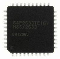
R5F61668RN50FPV Renesas Electronics America, R5F61668RN50FPV Datasheet - Page 1099

R5F61668RN50FPV
Manufacturer Part Number
R5F61668RN50FPV
Description
IC H8SX/1668 MCU FLASH 144LQFP
Manufacturer
Renesas Electronics America
Series
H8® H8SX/1600r
Datasheet
1.R5F61668RN50FPV.pdf
(1506 pages)
Specifications of R5F61668RN50FPV
Core Processor
H8SX
Core Size
16/32-Bit
Speed
50MHz
Connectivity
EBI/EMI, I²C, IrDA, SCI, SmartCard, USB
Peripherals
DMA, LVD, POR, PWM, WDT
Number Of I /o
92
Program Memory Size
1MB (1M x 8)
Program Memory Type
FLASH
Ram Size
56K x 8
Voltage - Supply (vcc/vdd)
3 V ~ 3.6 V
Data Converters
A/D 8x10b; D/A 2x8b
Oscillator Type
External
Operating Temperature
-20°C ~ 75°C
Package / Case
144-LQFP
For Use With
R0K561668S000BE - KIT STARTER FOR H8SX/1668R0K561664S001BE - KIT STARTER FOR H8SX/1651HS0005KCU11H - EMULATOR E10A-USB H8S(X),SH2(A)
Lead Free Status / RoHS Status
Lead free / RoHS Compliant
Eeprom Size
-
Available stocks
Company
Part Number
Manufacturer
Quantity
Price
Company:
Part Number:
R5F61668RN50FPV
Manufacturer:
Renesas Electronics America
Quantity:
10 000
- Current page: 1099 of 1506
- Download datasheet (9Mb)
Table 21.4 Time for Monitoring SCL
21.7
1. Confirm the ninth falling edge of the clock before issuing a stop or a repeated start condition.
2. The WAIT bit in the I
CKS3
0
1
The ninth falling edge can be confirmed by monitoring the SCLO bit in the I
register B (ICCRB).
If a stop or a repeated start condition is issued at certain timing in either of the following cases,
the stop or repeated start condition may be issued incorrectly.
The rising time of the SCL signal exceeds the time given in section 21.6, Bit Synchronous
The bit synchronous circuit is activated because a slave device holds the SCL bus low
If the WAIT bit is set to 1, when a slave device holds the SCL signal low more than one
transfer clock cycle during the eighth clock, the high level period of the ninth clock may be
shorter than a given period.
Circuit, because of the load on the SCL bus (load capacitance or pull-up resistance).
during the eighth clock.
Usage Notes
SCL monitor timing
reference clock
SCL
Internal SCL
Figure 21.18 Timing of the Bit Synchronous Circuit
CKS2
0
1
0
1
2
C bus mode register (ICMR) must be held 0.
Time for Monitoring SCL
7.5 tcyc
19.5 tcyc
17.5 tcyc
41.5 tcyc
V
IH
Rev. 2.00 Sep. 24, 2008 Page 1065 of 1468
Section 21 I
2
C Bus Interface 2 (IIC2)
2
C bus control
REJ09B0412-0200
Related parts for R5F61668RN50FPV
Image
Part Number
Description
Manufacturer
Datasheet
Request
R

Part Number:
Description:
KIT STARTER FOR M16C/29
Manufacturer:
Renesas Electronics America
Datasheet:

Part Number:
Description:
KIT STARTER FOR R8C/2D
Manufacturer:
Renesas Electronics America
Datasheet:

Part Number:
Description:
R0K33062P STARTER KIT
Manufacturer:
Renesas Electronics America
Datasheet:

Part Number:
Description:
KIT STARTER FOR R8C/23 E8A
Manufacturer:
Renesas Electronics America
Datasheet:

Part Number:
Description:
KIT STARTER FOR R8C/25
Manufacturer:
Renesas Electronics America
Datasheet:

Part Number:
Description:
KIT STARTER H8S2456 SHARPE DSPLY
Manufacturer:
Renesas Electronics America
Datasheet:

Part Number:
Description:
KIT STARTER FOR R8C38C
Manufacturer:
Renesas Electronics America
Datasheet:

Part Number:
Description:
KIT STARTER FOR R8C35C
Manufacturer:
Renesas Electronics America
Datasheet:

Part Number:
Description:
KIT STARTER FOR R8CL3AC+LCD APPS
Manufacturer:
Renesas Electronics America
Datasheet:

Part Number:
Description:
KIT STARTER FOR RX610
Manufacturer:
Renesas Electronics America
Datasheet:

Part Number:
Description:
KIT STARTER FOR R32C/118
Manufacturer:
Renesas Electronics America
Datasheet:

Part Number:
Description:
KIT DEV RSK-R8C/26-29
Manufacturer:
Renesas Electronics America
Datasheet:

Part Number:
Description:
KIT STARTER FOR SH7124
Manufacturer:
Renesas Electronics America
Datasheet:

Part Number:
Description:
KIT STARTER FOR H8SX/1622
Manufacturer:
Renesas Electronics America
Datasheet:

Part Number:
Description:
KIT DEV FOR SH7203
Manufacturer:
Renesas Electronics America
Datasheet:


