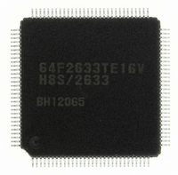
R5F61668RN50FPV Renesas Electronics America, R5F61668RN50FPV Datasheet - Page 1121

R5F61668RN50FPV
Manufacturer Part Number
R5F61668RN50FPV
Description
IC H8SX/1668 MCU FLASH 144LQFP
Manufacturer
Renesas Electronics America
Series
H8® H8SX/1600r
Datasheet
1.R5F61668RN50FPV.pdf
(1506 pages)
Specifications of R5F61668RN50FPV
Core Processor
H8SX
Core Size
16/32-Bit
Speed
50MHz
Connectivity
EBI/EMI, I²C, IrDA, SCI, SmartCard, USB
Peripherals
DMA, LVD, POR, PWM, WDT
Number Of I /o
92
Program Memory Size
1MB (1M x 8)
Program Memory Type
FLASH
Ram Size
56K x 8
Voltage - Supply (vcc/vdd)
3 V ~ 3.6 V
Data Converters
A/D 8x10b; D/A 2x8b
Oscillator Type
External
Operating Temperature
-20°C ~ 75°C
Package / Case
144-LQFP
For Use With
R0K561668S000BE - KIT STARTER FOR H8SX/1668R0K561664S001BE - KIT STARTER FOR H8SX/1651HS0005KCU11H - EMULATOR E10A-USB H8S(X),SH2(A)
Lead Free Status / RoHS Status
Lead free / RoHS Compliant
Eeprom Size
-
Available stocks
Company
Part Number
Manufacturer
Quantity
Price
Company:
Part Number:
R5F61668RN50FPV
Manufacturer:
Renesas Electronics America
Quantity:
10 000
- Current page: 1121 of 1506
- Download datasheet (9Mb)
Table 22.6 A/D Conversion Time (Scan Mode) (Unit 1)
22.4.4
A/D conversion can be externally triggered. For unit 0, an external trigger is input from the
ADTRG0 pin when the TRGS1, TRGS0, and EXTRGS bits are set to B'110 in ADCR_0. For unit
1, an external trigger is input from the ADTRG1 pin when the TRGS1, TRGS0, and EXTRGS bits
are set to B'110 in ADCR_1. A/D conversion starts when the ADST bit in ADCSR is set to 1 on
the falling edge of the ADTRG pin. Other operations, in both single and scan modes, are the same
as when the ADST bit has been set to 1 by software. Figure 22.7 shows the timing.
Also, A/D conversion for multiple units can be externally triggered (multiple units can start
simultaneously). For units 0 and 1, an external trigger is input from the ADTRG0 pin when the
TRGS1, TRGS0, and EXTRGS bits are set to B'111 in ADCR_0 and ADCR_1. A/D conversion
starts when the ADST bit in ADCSR is set to 1 on the falling edge of the ADTRG pin. The timing
is different from the one when multiple units do not start simultaneously. Figure 22.8 shows the
timing.
EXCKS
0
1
External Trigger Input Timing
CKS1
0
1
0
1
CKS0
0
1
0
1
0
1
0
1
512 (fixed)
256 (fixed)
128 (fixed)
64 (fixed)
320 (fixed)
160 (fixed)
80 (fixed)
40 (fixed)
Conversion Time (Number of States)
Rev. 2.00 Sep. 24, 2008 Page 1087 of 1468
Section 22 A/D Converter
REJ09B0412-0200
Related parts for R5F61668RN50FPV
Image
Part Number
Description
Manufacturer
Datasheet
Request
R

Part Number:
Description:
KIT STARTER FOR M16C/29
Manufacturer:
Renesas Electronics America
Datasheet:

Part Number:
Description:
KIT STARTER FOR R8C/2D
Manufacturer:
Renesas Electronics America
Datasheet:

Part Number:
Description:
R0K33062P STARTER KIT
Manufacturer:
Renesas Electronics America
Datasheet:

Part Number:
Description:
KIT STARTER FOR R8C/23 E8A
Manufacturer:
Renesas Electronics America
Datasheet:

Part Number:
Description:
KIT STARTER FOR R8C/25
Manufacturer:
Renesas Electronics America
Datasheet:

Part Number:
Description:
KIT STARTER H8S2456 SHARPE DSPLY
Manufacturer:
Renesas Electronics America
Datasheet:

Part Number:
Description:
KIT STARTER FOR R8C38C
Manufacturer:
Renesas Electronics America
Datasheet:

Part Number:
Description:
KIT STARTER FOR R8C35C
Manufacturer:
Renesas Electronics America
Datasheet:

Part Number:
Description:
KIT STARTER FOR R8CL3AC+LCD APPS
Manufacturer:
Renesas Electronics America
Datasheet:

Part Number:
Description:
KIT STARTER FOR RX610
Manufacturer:
Renesas Electronics America
Datasheet:

Part Number:
Description:
KIT STARTER FOR R32C/118
Manufacturer:
Renesas Electronics America
Datasheet:

Part Number:
Description:
KIT DEV RSK-R8C/26-29
Manufacturer:
Renesas Electronics America
Datasheet:

Part Number:
Description:
KIT STARTER FOR SH7124
Manufacturer:
Renesas Electronics America
Datasheet:

Part Number:
Description:
KIT STARTER FOR H8SX/1622
Manufacturer:
Renesas Electronics America
Datasheet:

Part Number:
Description:
KIT DEV FOR SH7203
Manufacturer:
Renesas Electronics America
Datasheet:


