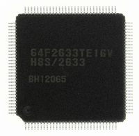
R5F61668RN50FPV Renesas Electronics America, R5F61668RN50FPV Datasheet - Page 1117

R5F61668RN50FPV
Manufacturer Part Number
R5F61668RN50FPV
Description
IC H8SX/1668 MCU FLASH 144LQFP
Manufacturer
Renesas Electronics America
Series
H8® H8SX/1600r
Datasheet
1.R5F61668RN50FPV.pdf
(1506 pages)
Specifications of R5F61668RN50FPV
Core Processor
H8SX
Core Size
16/32-Bit
Speed
50MHz
Connectivity
EBI/EMI, I²C, IrDA, SCI, SmartCard, USB
Peripherals
DMA, LVD, POR, PWM, WDT
Number Of I /o
92
Program Memory Size
1MB (1M x 8)
Program Memory Type
FLASH
Ram Size
56K x 8
Voltage - Supply (vcc/vdd)
3 V ~ 3.6 V
Data Converters
A/D 8x10b; D/A 2x8b
Oscillator Type
External
Operating Temperature
-20°C ~ 75°C
Package / Case
144-LQFP
For Use With
R0K561668S000BE - KIT STARTER FOR H8SX/1668R0K561664S001BE - KIT STARTER FOR H8SX/1651HS0005KCU11H - EMULATOR E10A-USB H8S(X),SH2(A)
Lead Free Status / RoHS Status
Lead free / RoHS Compliant
Eeprom Size
-
Available stocks
Company
Part Number
Manufacturer
Quantity
Price
Company:
Part Number:
R5F61668RN50FPV
Manufacturer:
Renesas Electronics America
Quantity:
10 000
- Current page: 1117 of 1506
- Download datasheet (9Mb)
2. When A/D conversion for each channel is completed, the A/D conversion result is sequentially
3. When A/D conversion of all selected channels is completed, the ADF bit in ADCSR is set to 1.
4. The ADST bit is not cleared automatically, and steps 2 to 3 are repeated as long as the ADST
Notes: 1. Consecutive A/D conversion on eight channels is only possible in unit 0.
ADST
ADF
Channel 0 (AN0)
operation state
Channel 1 (AN1)
operation state
Channel 2 (AN2)
operation state
Channel 3 (AN3)
operation state
ADDRA
ADDRB
ADDRC
ADDRD
When consecutive A/D conversion is performed on eight channels*
AN0 when CH3 = B'0.
transferred to the corresponding ADDR of each channel.
If the ADIE bit is set to 1 at this time, an ADI interrupt request is generated. A/D conversion of
the first channel in the group starts again.
bit remains set to 1. When the ADST bit is cleared to 0, A/D conversion stops and the A/D
converter enters wait state. If the ADST bit is later set to 1, A/D conversion starts again from
the first channel in the group.
2. As conversion start trigger, units 0 and 1 of TMR, and units 2 and 3 of TMR are
Notes: 1.
available in unit 0, and unit 1, respectively.
2.
(Continuous Scan Mode, Three Channels (AN0 to AN2) Selected)
↓ indicates the timing of instruction execution by software.
Data being converted is ignored.
Waiting for
conversion
Waiting for conversion
Waiting for conversion
Waiting for conversion
Figure 22.4 Example of A/D Conversion
Set *
A/D
conver-
sion 1
1
Transfer
A/D conversion consecutive execution
A/D
conver-
sion 2
Waiting for conversion
A/D conversion result 1
A/D
conver-
sion 3
Waiting for conversion
Rev. 2.00 Sep. 24, 2008 Page 1083 of 1468
A/D conversion time
A/D
conver-
sion 4
A/D conversion result 2
1
, A/D conversion starts on
A/D conversion result 3
A/D
conver-
sion 5
Section 22 A/D Converter
A/D conversion result 4
Waiting for conversion
Waiting for conversion
*
Clear *
2
REJ09B0412-0200
Waiting for
conversion
1
Clear *
1
Related parts for R5F61668RN50FPV
Image
Part Number
Description
Manufacturer
Datasheet
Request
R

Part Number:
Description:
KIT STARTER FOR M16C/29
Manufacturer:
Renesas Electronics America
Datasheet:

Part Number:
Description:
KIT STARTER FOR R8C/2D
Manufacturer:
Renesas Electronics America
Datasheet:

Part Number:
Description:
R0K33062P STARTER KIT
Manufacturer:
Renesas Electronics America
Datasheet:

Part Number:
Description:
KIT STARTER FOR R8C/23 E8A
Manufacturer:
Renesas Electronics America
Datasheet:

Part Number:
Description:
KIT STARTER FOR R8C/25
Manufacturer:
Renesas Electronics America
Datasheet:

Part Number:
Description:
KIT STARTER H8S2456 SHARPE DSPLY
Manufacturer:
Renesas Electronics America
Datasheet:

Part Number:
Description:
KIT STARTER FOR R8C38C
Manufacturer:
Renesas Electronics America
Datasheet:

Part Number:
Description:
KIT STARTER FOR R8C35C
Manufacturer:
Renesas Electronics America
Datasheet:

Part Number:
Description:
KIT STARTER FOR R8CL3AC+LCD APPS
Manufacturer:
Renesas Electronics America
Datasheet:

Part Number:
Description:
KIT STARTER FOR RX610
Manufacturer:
Renesas Electronics America
Datasheet:

Part Number:
Description:
KIT STARTER FOR R32C/118
Manufacturer:
Renesas Electronics America
Datasheet:

Part Number:
Description:
KIT DEV RSK-R8C/26-29
Manufacturer:
Renesas Electronics America
Datasheet:

Part Number:
Description:
KIT STARTER FOR SH7124
Manufacturer:
Renesas Electronics America
Datasheet:

Part Number:
Description:
KIT STARTER FOR H8SX/1622
Manufacturer:
Renesas Electronics America
Datasheet:

Part Number:
Description:
KIT DEV FOR SH7203
Manufacturer:
Renesas Electronics America
Datasheet:


