R5F61668RN50FPV Renesas Electronics America, R5F61668RN50FPV Datasheet - Page 1476
R5F61668RN50FPV
Manufacturer Part Number
R5F61668RN50FPV
Description
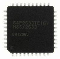
IC H8SX/1668 MCU FLASH 144LQFP
Manufacturer
Renesas Electronics America
Series
H8® H8SX/1600r
Datasheet
1.R5F61668RN50FPV.pdf
(1506 pages)
Specifications of R5F61668RN50FPV
Core Processor
H8SX
Core Size
16/32-Bit
Speed
50MHz
Connectivity
EBI/EMI, I²C, IrDA, SCI, SmartCard, USB
Peripherals
DMA, LVD, POR, PWM, WDT
Number Of I /o
92
Program Memory Size
1MB (1M x 8)
Program Memory Type
FLASH
Ram Size
56K x 8
Voltage - Supply (vcc/vdd)
3 V ~ 3.6 V
Data Converters
A/D 8x10b; D/A 2x8b
Oscillator Type
External
Operating Temperature
-20°C ~ 75°C
Package / Case
144-LQFP
For Use With
R0K561668S000BE - KIT STARTER FOR H8SX/1668R0K561664S001BE - KIT STARTER FOR H8SX/1651HS0005KCU11H - EMULATOR E10A-USB H8S(X),SH2(A)
Lead Free Status / RoHS Status
Lead free / RoHS Compliant
Eeprom Size
-
Available stocks
Company
Part Number
Manufacturer
Quantity
Price
Company:

Part Number:
R5F61668RN50FPV
Manufacturer:
Renesas Electronics America
Quantity:
10 000


Main Revisions and Additions in this Edition
Rev. 2.00 Sep. 24, 2008 Page 1442 of 1468
REJ09B0412-0200
Item
Section 25 Flash Memory
25.7.1 Programming/Erasing
Interface Registers
25.7.2 Programming/Erasing
Interface Parameters
(3) Flash Program/Erase
Frequency Parameter
(FPEFEQ)
25.14 Usage Notes
Section 26 Boundary Scan
26.4.3 Boundary Scan
Register (JTBSR)
Section 27 Clock Pulse
Generator
27.6.1 Notes on Clock Pulse
Generator
Section 28 Power-Down
Modes
28.2 Register Descriptions
Page
1120
1132
1203
1210
1231
1239
Revision (See Manual for Details)
Added
Bit 0 R/W*
Note: This is a write-only bit. This bit is always read as 0.
Amended
FPEFEQ sets the operating frequency of the CPU. The
operating frequency available in this LSI ranges from 8 MHz
to 50 MHz.
Amended
5. Do not turn off the Vcc power supply nor remove the chip
Amended
7. At powering on the Vcc power supply, fix the RES pin to
Amended
Table 26.4
Table item "from TDI" is added.
"from TDI" and "to TDO" are deleted from the pin name of
the table item
Amended
Item numbers 1 to 5 are added
4. Note that the frequency of f will be changed in the middle
of a bus cycle when setting SCKCR0 or SUBCKCR while
executing the external bus cycle with the write-data-buffer
function and EXDMAC
Amended
•
from the PROM programmer during programming/erasure
in which a high voltage is applied to the flash memory.
Doing so may damage the flash memory permanently. If
a reset is input, the reset must be released after the reset
input period of at least 100µs.
low and set the flash memory to hardware protection
state. This power on timing must also be satisfied at a
power-off and power-on caused by a power failure and
other factors.
Deep standby backup register n (DPSBKRn)
(n=15 to 0)
Related parts for R5F61668RN50FPV
Image
Part Number
Description
Manufacturer
Datasheet
Request
R

Part Number:
Description:
KIT STARTER FOR M16C/29
Manufacturer:
Renesas Electronics America
Datasheet:

Part Number:
Description:
KIT STARTER FOR R8C/2D
Manufacturer:
Renesas Electronics America
Datasheet:

Part Number:
Description:
R0K33062P STARTER KIT
Manufacturer:
Renesas Electronics America
Datasheet:

Part Number:
Description:
KIT STARTER FOR R8C/23 E8A
Manufacturer:
Renesas Electronics America
Datasheet:

Part Number:
Description:
KIT STARTER FOR R8C/25
Manufacturer:
Renesas Electronics America
Datasheet:

Part Number:
Description:
KIT STARTER H8S2456 SHARPE DSPLY
Manufacturer:
Renesas Electronics America
Datasheet:

Part Number:
Description:
KIT STARTER FOR R8C38C
Manufacturer:
Renesas Electronics America
Datasheet:

Part Number:
Description:
KIT STARTER FOR R8C35C
Manufacturer:
Renesas Electronics America
Datasheet:

Part Number:
Description:
KIT STARTER FOR R8CL3AC+LCD APPS
Manufacturer:
Renesas Electronics America
Datasheet:
Part Number:
Description:
KIT STARTER FOR RX610
Manufacturer:
Renesas Electronics America
Datasheet:

Part Number:
Description:
KIT STARTER FOR R32C/118
Manufacturer:
Renesas Electronics America
Datasheet:

Part Number:
Description:
KIT DEV RSK-R8C/26-29
Manufacturer:
Renesas Electronics America
Datasheet:

Part Number:
Description:
KIT STARTER FOR SH7124
Manufacturer:
Renesas Electronics America
Datasheet:

Part Number:
Description:
KIT STARTER FOR H8SX/1622
Manufacturer:
Renesas Electronics America
Datasheet:

Part Number:
Description:
KIT DEV FOR SH7203
Manufacturer:
Renesas Electronics America
Datasheet: