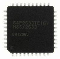
R5F61668RN50FPV Renesas Electronics America, R5F61668RN50FPV Datasheet - Page 58

R5F61668RN50FPV
Manufacturer Part Number
R5F61668RN50FPV
Description
IC H8SX/1668 MCU FLASH 144LQFP
Manufacturer
Renesas Electronics America
Series
H8® H8SX/1600r
Datasheet
1.R5F61668RN50FPV.pdf
(1506 pages)
Specifications of R5F61668RN50FPV
Core Processor
H8SX
Core Size
16/32-Bit
Speed
50MHz
Connectivity
EBI/EMI, I²C, IrDA, SCI, SmartCard, USB
Peripherals
DMA, LVD, POR, PWM, WDT
Number Of I /o
92
Program Memory Size
1MB (1M x 8)
Program Memory Type
FLASH
Ram Size
56K x 8
Voltage - Supply (vcc/vdd)
3 V ~ 3.6 V
Data Converters
A/D 8x10b; D/A 2x8b
Oscillator Type
External
Operating Temperature
-20°C ~ 75°C
Package / Case
144-LQFP
For Use With
R0K561668S000BE - KIT STARTER FOR H8SX/1668R0K561664S001BE - KIT STARTER FOR H8SX/1651HS0005KCU11H - EMULATOR E10A-USB H8S(X),SH2(A)
Lead Free Status / RoHS Status
Lead free / RoHS Compliant
Eeprom Size
-
Available stocks
Company
Part Number
Manufacturer
Quantity
Price
Company:
Part Number:
R5F61668RN50FPV
Manufacturer:
Renesas Electronics America
Quantity:
10 000
- Current page: 58 of 1506
- Download datasheet (9Mb)
Section 1 Overview
Classification
Address bus
Data bus
Bus control
Rev. 2.00 Sep. 24, 2008 Page 24 of 1468
REJ09B0412-0200
Pin Name
A23 to A0
D15 to D0
BREQ
BREQO
BACK
BS-A/BS-B
AS
AH
RD
RD/WR-A/RD/WR-B Output
LHWR
LLWR
LUB
LLB
I/O
Output
Input/
output
Input
Output
Output
Output
Output
Output
Output
Output
Output
Output
Output
Description
External bus-master modules assert this signal to request
Output pins for the address bits.
Input and output for the bidirectional data bus. These pins
also output addresses when accessing an address–data
multiplexed I/O interface space.
the bus.
Internal bus-master modules assert this signal to request
access to the external space via the bus in the external bus
released state.
Bus acknowledge signal, which indicates that the bus has
been released.
Indicates the start of a bus cycle.
Strobe signal which indicates that the output address on the
address bus is valid in access to the basic bus interface or
byte control SRAM interface space.
This signal is used to hold the address when accessing the
address-data multiplexed I/O interface space.
Strobe signal which indicates that reading from the basic bus
interface space is in progress.
Indicates the direction (input or output) of the data bus.
Strobe signal which indicates that the higher-order byte (D15
to D8) is valid in access to the basic bus interface space.
Strobe signal which indicates that the lower-order byte (D7 to
D0) is valid in access to the basic bus interface space.
Strobe signal which indicates that the higher-order byte (D15
to D8) is valid in access to the byte control SRAM interface
space.
Strobe signal which indicates that the lower-order byte (D7 to
D0) is valid in access to the byte control SRAM interface
space.
Related parts for R5F61668RN50FPV
Image
Part Number
Description
Manufacturer
Datasheet
Request
R

Part Number:
Description:
KIT STARTER FOR M16C/29
Manufacturer:
Renesas Electronics America
Datasheet:

Part Number:
Description:
KIT STARTER FOR R8C/2D
Manufacturer:
Renesas Electronics America
Datasheet:

Part Number:
Description:
R0K33062P STARTER KIT
Manufacturer:
Renesas Electronics America
Datasheet:

Part Number:
Description:
KIT STARTER FOR R8C/23 E8A
Manufacturer:
Renesas Electronics America
Datasheet:

Part Number:
Description:
KIT STARTER FOR R8C/25
Manufacturer:
Renesas Electronics America
Datasheet:

Part Number:
Description:
KIT STARTER H8S2456 SHARPE DSPLY
Manufacturer:
Renesas Electronics America
Datasheet:

Part Number:
Description:
KIT STARTER FOR R8C38C
Manufacturer:
Renesas Electronics America
Datasheet:

Part Number:
Description:
KIT STARTER FOR R8C35C
Manufacturer:
Renesas Electronics America
Datasheet:

Part Number:
Description:
KIT STARTER FOR R8CL3AC+LCD APPS
Manufacturer:
Renesas Electronics America
Datasheet:

Part Number:
Description:
KIT STARTER FOR RX610
Manufacturer:
Renesas Electronics America
Datasheet:

Part Number:
Description:
KIT STARTER FOR R32C/118
Manufacturer:
Renesas Electronics America
Datasheet:

Part Number:
Description:
KIT DEV RSK-R8C/26-29
Manufacturer:
Renesas Electronics America
Datasheet:

Part Number:
Description:
KIT STARTER FOR SH7124
Manufacturer:
Renesas Electronics America
Datasheet:

Part Number:
Description:
KIT STARTER FOR H8SX/1622
Manufacturer:
Renesas Electronics America
Datasheet:

Part Number:
Description:
KIT DEV FOR SH7203
Manufacturer:
Renesas Electronics America
Datasheet:


