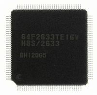
R5F61668RN50FPV Renesas Electronics America, R5F61668RN50FPV Datasheet - Page 441

R5F61668RN50FPV
Manufacturer Part Number
R5F61668RN50FPV
Description
IC H8SX/1668 MCU FLASH 144LQFP
Manufacturer
Renesas Electronics America
Series
H8® H8SX/1600r
Datasheet
1.R5F61668RN50FPV.pdf
(1506 pages)
Specifications of R5F61668RN50FPV
Core Processor
H8SX
Core Size
16/32-Bit
Speed
50MHz
Connectivity
EBI/EMI, I²C, IrDA, SCI, SmartCard, USB
Peripherals
DMA, LVD, POR, PWM, WDT
Number Of I /o
92
Program Memory Size
1MB (1M x 8)
Program Memory Type
FLASH
Ram Size
56K x 8
Voltage - Supply (vcc/vdd)
3 V ~ 3.6 V
Data Converters
A/D 8x10b; D/A 2x8b
Oscillator Type
External
Operating Temperature
-20°C ~ 75°C
Package / Case
144-LQFP
For Use With
R0K561668S000BE - KIT STARTER FOR H8SX/1668R0K561664S001BE - KIT STARTER FOR H8SX/1651HS0005KCU11H - EMULATOR E10A-USB H8S(X),SH2(A)
Lead Free Status / RoHS Status
Lead free / RoHS Compliant
Eeprom Size
-
Available stocks
Company
Part Number
Manufacturer
Quantity
Price
Company:
Part Number:
R5F61668RN50FPV
Manufacturer:
Renesas Electronics America
Quantity:
10 000
- Current page: 441 of 1506
- Download datasheet (9Mb)
Section 10 DMA Controller (DMAC)
(2)
Repeat Transfer Mode
In repeat transfer mode, one data access size of data is transferred at a single transfer request. Up
to 4 Gbytes can be specified as a total transfer size by DTCR. The repeat size can be specified in
DBSR up to 65536 × data access size.
The repeat area can be specified for the source or destination address side by bits ARS1 and ARS0
in DACR. The address specified as the repeat area returns to the transfer start address when the
repeat size of transfers is completed. This operation is repeated until the total transfer size
specified in DTCR is completed. When H'00000000 is specified in DTCR, it is regarded as the
free running mode and repeat transfer is continued until the DTE bit in DMDR is cleared to 0.
In addition, a DMA transfer can be stopped and a repeat size end interrupt can be requested to the
CPU or DTC when the repeat size of transfers is completed. When the next transfer is requested
after completion of a 1-repeat size data transfer while the RPTIE bit is set to 1, the DTE bit in
DMDR is cleared to 0 and the ESIF bit in DMDR is set to 1 to complete the transfer. At this time,
an interrupt is requested to the CPU or DTC when the ESIE bit in DMDR is set to 1.
The timing of the TEND signals is the same as in normal transfer mode.
Figure 10.9 shows the operation in repeat transfer mode while dual address mode is set.
When the repeat area is specified as neither source nor destination address side, the operation is
the same as the normal transfer mode operation shown in figure 10.8. In this case, a repeat size
end interrupt can also be requested to the CPU when the repeat size of transfers is completed.
Rev. 2.00 Sep. 24, 2008 Page 407 of 1468
REJ09B0412-0200
Related parts for R5F61668RN50FPV
Image
Part Number
Description
Manufacturer
Datasheet
Request
R

Part Number:
Description:
KIT STARTER FOR M16C/29
Manufacturer:
Renesas Electronics America
Datasheet:

Part Number:
Description:
KIT STARTER FOR R8C/2D
Manufacturer:
Renesas Electronics America
Datasheet:

Part Number:
Description:
R0K33062P STARTER KIT
Manufacturer:
Renesas Electronics America
Datasheet:

Part Number:
Description:
KIT STARTER FOR R8C/23 E8A
Manufacturer:
Renesas Electronics America
Datasheet:

Part Number:
Description:
KIT STARTER FOR R8C/25
Manufacturer:
Renesas Electronics America
Datasheet:

Part Number:
Description:
KIT STARTER H8S2456 SHARPE DSPLY
Manufacturer:
Renesas Electronics America
Datasheet:

Part Number:
Description:
KIT STARTER FOR R8C38C
Manufacturer:
Renesas Electronics America
Datasheet:

Part Number:
Description:
KIT STARTER FOR R8C35C
Manufacturer:
Renesas Electronics America
Datasheet:

Part Number:
Description:
KIT STARTER FOR R8CL3AC+LCD APPS
Manufacturer:
Renesas Electronics America
Datasheet:

Part Number:
Description:
KIT STARTER FOR RX610
Manufacturer:
Renesas Electronics America
Datasheet:

Part Number:
Description:
KIT STARTER FOR R32C/118
Manufacturer:
Renesas Electronics America
Datasheet:

Part Number:
Description:
KIT DEV RSK-R8C/26-29
Manufacturer:
Renesas Electronics America
Datasheet:

Part Number:
Description:
KIT STARTER FOR SH7124
Manufacturer:
Renesas Electronics America
Datasheet:

Part Number:
Description:
KIT STARTER FOR H8SX/1622
Manufacturer:
Renesas Electronics America
Datasheet:

Part Number:
Description:
KIT DEV FOR SH7203
Manufacturer:
Renesas Electronics America
Datasheet:


