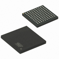
ATSAM3U4CA-CU Atmel, ATSAM3U4CA-CU Datasheet - Page 1062

ATSAM3U4CA-CU
Manufacturer Part Number
ATSAM3U4CA-CU
Description
IC MCU 32BIT 256KB FLSH 100TFBGA
Manufacturer
Atmel
Series
SAM3Ur
Specifications of ATSAM3U4CA-CU
Core Processor
ARM® Cortex-M3™
Core Size
32-Bit
Speed
96MHz
Connectivity
EBI/EMI, I²C, MMC, SPI, SSC, UART/USART, USB
Peripherals
Brown-out Detect/Reset, DMA, I²S, POR, PWM, WDT
Number Of I /o
57
Program Memory Size
256KB (256K x 8)
Program Memory Type
FLASH
Ram Size
52K x 8
Voltage - Supply (vcc/vdd)
1.65 V ~ 1.95 V
Data Converters
A/D 4x10b, 4x12b
Oscillator Type
Internal
Operating Temperature
-40°C ~ 85°C
Package / Case
100-TFBGA
Processor Series
ATSAM3x
Core
ARM Cortex M3
Data Bus Width
32 bit
Data Ram Size
52 KB
Interface Type
3xUSART, TWI, 4xSPI, Bus
Maximum Clock Frequency
96 MHz
Number Of Programmable I/os
57
Number Of Timers
8
Operating Supply Voltage
1.62 V to 3.6 V
Maximum Operating Temperature
+ 85 C
Mounting Style
SMD/SMT
3rd Party Development Tools
JTRACE-CM3, MDK-ARM, RL-ARM, ULINK2
Development Tools By Supplier
ATSAM3U-EK
Minimum Operating Temperature
- 40 C
Lead Free Status / RoHS Status
Lead free / RoHS Compliant
Eeprom Size
-
Lead Free Status / Rohs Status
Lead free / RoHS Compliant
Available stocks
Company
Part Number
Manufacturer
Quantity
Price
Part Number:
ATSAM3U4CA-CU
Manufacturer:
ATMEL/爱特梅尔
Quantity:
20 000
- Current page: 1062 of 1171
- Download datasheet (25Mb)
41.5.8
41.5.9
1062
SAM3U Series
Conversion Triggers
Sleep Mode and Conversion Sequencer
Conversions of the active analog channels are started with a software or a hardware trigger. The
software trigger is provided by writing the Control Register (ADC12B_CR) with the START bit at
1.
The hardware trigger can be one of the TIOA outputs of the Timer Counter channels, PWM
Event lines or the external trigger input of the ADC12B (AD12BTRG). The hardware trigger is
selected with the field TRGSEL in the Mode Register (ADC12B_MR). The selected hardware
trigger is enabled with the TRGEN bit in the Mode Register (ADC12B_MR).
If a hardware trigger is selected, the start of a conversion is triggered after a delay starting at
each rising edge of the selected signal. Due to asynchronous handling, the delay may vary in a
range of 2 MCK clock periods to 1 ADC12B clock period.
If one of the TIOA outputs is selected, the corresponding Timer Counter channel must be pro-
grammed in Waveform Mode.
Only one start command is necessary to initiate a conversion sequence on all the channels. The
ADC12B hardware logic automatically performs the conversions on the active channels, then
waits for a new request. The Channel Enable (ADC12B_CHER) and Channel Disable
(ADC12B_CHDR) Registers enable the analog channels to be enabled or disabled
independently.
If the ADC12B is used with a PDC, only the transfers of converted data from enabled channels
are performed and the resulting data buffers should be interpreted accordingly.
Warning: Enabling hardware triggers does not disable the software trigger functionality. Thus, if
a hardware trigger is selected, the start of a conversion can be initiated either by the hardware or
the software trigger.
The ADC12B Sleep Mode maximizes power saving by automatically deactivating the ADC12B
when it is not being used for conversions. Sleep Mode is selected by setting the SLEEP bit in the
Mode Register ADC12B_MR.
Two sleep Mode are selectable (OFFMODES): STANDBY Mode and OFF Mode. In Standby
Mode, the ADC12B is powered off except voltage reference to allow fast startup. In OFF Mode
the ADC12B is totally powered off.
Table 41-8.
The SLEEP mode is automatically managed by a conversion sequencer, which can automati-
cally process the conversions of all channels at lowest power consumption.
SLEEP Bit
0
1
1
Low Power Modes According SLEEP Bit and OFFMODES Bit.
OFFMODES Bit
trigger
start
_
0
1
delay
Low Power Mode
Standby Mode
Normal Mode
Off Mode
6430D–ATARM–25-Mar-11
Related parts for ATSAM3U4CA-CU
Image
Part Number
Description
Manufacturer
Datasheet
Request
R

Part Number:
Description:
KIT EVAL FOR AT91SAM3U CORTEX
Manufacturer:
Atmel
Datasheet:

Part Number:
Description:
AT91 ARM Thumb-based Microcontrollers
Manufacturer:
ATMEL [ATMEL Corporation]
Datasheet:

Part Number:
Description:
DEV KIT FOR AVR/AVR32
Manufacturer:
Atmel
Datasheet:

Part Number:
Description:
INTERVAL AND WIPE/WASH WIPER CONTROL IC WITH DELAY
Manufacturer:
ATMEL Corporation
Datasheet:

Part Number:
Description:
Low-Voltage Voice-Switched IC for Hands-Free Operation
Manufacturer:
ATMEL Corporation
Datasheet:

Part Number:
Description:
MONOLITHIC INTEGRATED FEATUREPHONE CIRCUIT
Manufacturer:
ATMEL Corporation
Datasheet:

Part Number:
Description:
AM-FM Receiver IC U4255BM-M
Manufacturer:
ATMEL Corporation
Datasheet:

Part Number:
Description:
Monolithic Integrated Feature Phone Circuit
Manufacturer:
ATMEL Corporation
Datasheet:

Part Number:
Description:
Multistandard Video-IF and Quasi Parallel Sound Processing
Manufacturer:
ATMEL Corporation
Datasheet:

Part Number:
Description:
High-performance EE PLD
Manufacturer:
ATMEL Corporation
Datasheet:

Part Number:
Description:
8-bit Flash Microcontroller
Manufacturer:
ATMEL Corporation
Datasheet:

Part Number:
Description:
2-Wire Serial EEPROM
Manufacturer:
ATMEL Corporation
Datasheet:


