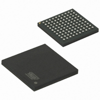
ATSAM3U4CA-CU Atmel, ATSAM3U4CA-CU Datasheet - Page 1063

ATSAM3U4CA-CU
Manufacturer Part Number
ATSAM3U4CA-CU
Description
IC MCU 32BIT 256KB FLSH 100TFBGA
Manufacturer
Atmel
Series
SAM3Ur
Specifications of ATSAM3U4CA-CU
Core Processor
ARM® Cortex-M3™
Core Size
32-Bit
Speed
96MHz
Connectivity
EBI/EMI, I²C, MMC, SPI, SSC, UART/USART, USB
Peripherals
Brown-out Detect/Reset, DMA, I²S, POR, PWM, WDT
Number Of I /o
57
Program Memory Size
256KB (256K x 8)
Program Memory Type
FLASH
Ram Size
52K x 8
Voltage - Supply (vcc/vdd)
1.65 V ~ 1.95 V
Data Converters
A/D 4x10b, 4x12b
Oscillator Type
Internal
Operating Temperature
-40°C ~ 85°C
Package / Case
100-TFBGA
Processor Series
ATSAM3x
Core
ARM Cortex M3
Data Bus Width
32 bit
Data Ram Size
52 KB
Interface Type
3xUSART, TWI, 4xSPI, Bus
Maximum Clock Frequency
96 MHz
Number Of Programmable I/os
57
Number Of Timers
8
Operating Supply Voltage
1.62 V to 3.6 V
Maximum Operating Temperature
+ 85 C
Mounting Style
SMD/SMT
3rd Party Development Tools
JTRACE-CM3, MDK-ARM, RL-ARM, ULINK2
Development Tools By Supplier
ATSAM3U-EK
Minimum Operating Temperature
- 40 C
Lead Free Status / RoHS Status
Lead free / RoHS Compliant
Eeprom Size
-
Lead Free Status / Rohs Status
Lead free / RoHS Compliant
Available stocks
Company
Part Number
Manufacturer
Quantity
Price
Part Number:
ATSAM3U4CA-CU
Manufacturer:
ATMEL/爱特梅尔
Quantity:
20 000
- Current page: 1063 of 1171
- Download datasheet (25Mb)
41.5.10
6430D–ATARM–25-Mar-11
ADC12B Timings
When a start conversion request occurs, the ADC12B is automatically activated. As the analog
cell requires a start-up time, the logic waits during this time and starts the conversion on the
enabled channels. When all conversions are complete, the ADC12B is deactivated until the next
trigger. Triggers occurring during the sequence are not taken into account.
The conversion sequencer allows automatic processing with minimum processor intervention
and optimized power consumption. Conversion sequences can be performed periodically using
a Timer/Counter output or a PWM Event line. The periodic acquisition of several samples can be
processed automatically without any intervention of the processor thanks to the PDC.
The conversion sequencer can only be used if all ADC12B inputs have the same input configu-
ration, e.g. same PGA gain, same input type (differential or single ended) and same input offset.
If input have different configurations, sequencer can’t be used because PGA gain, input type
and input offset can’t be changed.
Note:
Each ADC12B has its own minimal Startup Time that is programmed through the field
STARTUP in the Mode Register (ADC12B_MR).
In the same way, a minimal Sample and Hold Time is necessary for the ADC12B to guarantee
the best converted final value between the two channels selection. This time has to be pro-
grammed through the SHTIM bitfield in the Mode Register (ADC12B_MR).
Warning: No input buffer amplifier to isolate the source is included in the ADC12B. This must be
taken into consideration to program a precise value in the SHTIM field. See the section, ADC12B
Characteristics in the product datasheet.
The reference voltage pins always remain connected in normal mode as in sleep mode.
SAM3U Series
1063
Related parts for ATSAM3U4CA-CU
Image
Part Number
Description
Manufacturer
Datasheet
Request
R

Part Number:
Description:
KIT EVAL FOR AT91SAM3U CORTEX
Manufacturer:
Atmel
Datasheet:

Part Number:
Description:
AT91 ARM Thumb-based Microcontrollers
Manufacturer:
ATMEL [ATMEL Corporation]
Datasheet:

Part Number:
Description:
DEV KIT FOR AVR/AVR32
Manufacturer:
Atmel
Datasheet:

Part Number:
Description:
INTERVAL AND WIPE/WASH WIPER CONTROL IC WITH DELAY
Manufacturer:
ATMEL Corporation
Datasheet:

Part Number:
Description:
Low-Voltage Voice-Switched IC for Hands-Free Operation
Manufacturer:
ATMEL Corporation
Datasheet:

Part Number:
Description:
MONOLITHIC INTEGRATED FEATUREPHONE CIRCUIT
Manufacturer:
ATMEL Corporation
Datasheet:

Part Number:
Description:
AM-FM Receiver IC U4255BM-M
Manufacturer:
ATMEL Corporation
Datasheet:

Part Number:
Description:
Monolithic Integrated Feature Phone Circuit
Manufacturer:
ATMEL Corporation
Datasheet:

Part Number:
Description:
Multistandard Video-IF and Quasi Parallel Sound Processing
Manufacturer:
ATMEL Corporation
Datasheet:

Part Number:
Description:
High-performance EE PLD
Manufacturer:
ATMEL Corporation
Datasheet:

Part Number:
Description:
8-bit Flash Microcontroller
Manufacturer:
ATMEL Corporation
Datasheet:

Part Number:
Description:
2-Wire Serial EEPROM
Manufacturer:
ATMEL Corporation
Datasheet:


