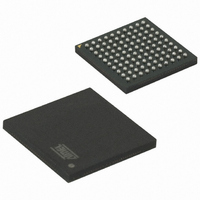
ATSAM3U4CA-CU Atmel, ATSAM3U4CA-CU Datasheet - Page 328

ATSAM3U4CA-CU
Manufacturer Part Number
ATSAM3U4CA-CU
Description
IC MCU 32BIT 256KB FLSH 100TFBGA
Manufacturer
Atmel
Series
SAM3Ur
Specifications of ATSAM3U4CA-CU
Core Processor
ARM® Cortex-M3™
Core Size
32-Bit
Speed
96MHz
Connectivity
EBI/EMI, I²C, MMC, SPI, SSC, UART/USART, USB
Peripherals
Brown-out Detect/Reset, DMA, I²S, POR, PWM, WDT
Number Of I /o
57
Program Memory Size
256KB (256K x 8)
Program Memory Type
FLASH
Ram Size
52K x 8
Voltage - Supply (vcc/vdd)
1.65 V ~ 1.95 V
Data Converters
A/D 4x10b, 4x12b
Oscillator Type
Internal
Operating Temperature
-40°C ~ 85°C
Package / Case
100-TFBGA
Processor Series
ATSAM3x
Core
ARM Cortex M3
Data Bus Width
32 bit
Data Ram Size
52 KB
Interface Type
3xUSART, TWI, 4xSPI, Bus
Maximum Clock Frequency
96 MHz
Number Of Programmable I/os
57
Number Of Timers
8
Operating Supply Voltage
1.62 V to 3.6 V
Maximum Operating Temperature
+ 85 C
Mounting Style
SMD/SMT
3rd Party Development Tools
JTRACE-CM3, MDK-ARM, RL-ARM, ULINK2
Development Tools By Supplier
ATSAM3U-EK
Minimum Operating Temperature
- 40 C
Lead Free Status / RoHS Status
Lead free / RoHS Compliant
Eeprom Size
-
Lead Free Status / Rohs Status
Lead free / RoHS Compliant
Available stocks
Company
Part Number
Manufacturer
Quantity
Price
Part Number:
ATSAM3U4CA-CU
Manufacturer:
ATMEL/爱特梅尔
Quantity:
20 000
- Current page: 328 of 1171
- Download datasheet (25Mb)
22.2.5.1
22.2.5.2
328
SAM3U Series
Flash Read Command
Flash Write Command
This command is used to read the contents of the Flash memory. The read command can start
at any valid address in the memory plane and is optimized for consecutive reads. Read hand-
shaking can be chained; an internal address buffer is automatically increased.
Table 22-6.
This command is used to write the Flash contents.
The Flash memory plane is organized into several pages. Data to be written are stored in a load
buffer that corresponds to a Flash memory page. The load buffer is automatically flushed to the
Flash:
The Write Page command (WP) is optimized for consecutive writes. Write handshaking can be
chained; an internal address buffer is automatically increased.
Table 22-7.
Step
1
2
3
4
5
...
n
n+1
n+2
n+3
...
Step
1
2
3
4
5
...
n
n+1
• before access to any page other than the current one
• when a new command is validated (MODE = CMDE)
Handshake Sequence
Write handshaking
Write handshaking
Write handshaking
Read handshaking
Read handshaking
...
Write handshaking
Write handshaking
Read handshaking
Read handshaking
...
Handshake Sequence
Write handshaking
Write handshaking
Write handshaking
Write handshaking
Write handshaking
...
Write handshaking
Write handshaking
Read Command
Write Command
MODE[3:0]
CMDE
ADDR0
ADDR1
DATA
DATA
...
ADDR0
ADDR1
MODE[3:0]
CMDE
ADDR0
ADDR1
DATA
DATA
...
ADDR0
ADDR1
DATA
DATA
...
DATA[15:0]
READ
Memory Address LSB
Memory Address
*Memory Address++
*Memory Address++
...
Memory Address
*Memory Address++
*Memory Address++
...
DATA[15:0]
WP or WPL or EWP or EWPL
Memory Address LSB
Memory Address
*Memory Address++
*Memory Address++
...
Memory Address LSB
Memory Address
Memory Address LSB
6430D–ATARM–25-Mar-11
Related parts for ATSAM3U4CA-CU
Image
Part Number
Description
Manufacturer
Datasheet
Request
R

Part Number:
Description:
KIT EVAL FOR AT91SAM3U CORTEX
Manufacturer:
Atmel
Datasheet:

Part Number:
Description:
AT91 ARM Thumb-based Microcontrollers
Manufacturer:
ATMEL [ATMEL Corporation]
Datasheet:

Part Number:
Description:
DEV KIT FOR AVR/AVR32
Manufacturer:
Atmel
Datasheet:

Part Number:
Description:
INTERVAL AND WIPE/WASH WIPER CONTROL IC WITH DELAY
Manufacturer:
ATMEL Corporation
Datasheet:

Part Number:
Description:
Low-Voltage Voice-Switched IC for Hands-Free Operation
Manufacturer:
ATMEL Corporation
Datasheet:

Part Number:
Description:
MONOLITHIC INTEGRATED FEATUREPHONE CIRCUIT
Manufacturer:
ATMEL Corporation
Datasheet:

Part Number:
Description:
AM-FM Receiver IC U4255BM-M
Manufacturer:
ATMEL Corporation
Datasheet:

Part Number:
Description:
Monolithic Integrated Feature Phone Circuit
Manufacturer:
ATMEL Corporation
Datasheet:

Part Number:
Description:
Multistandard Video-IF and Quasi Parallel Sound Processing
Manufacturer:
ATMEL Corporation
Datasheet:

Part Number:
Description:
High-performance EE PLD
Manufacturer:
ATMEL Corporation
Datasheet:

Part Number:
Description:
8-bit Flash Microcontroller
Manufacturer:
ATMEL Corporation
Datasheet:

Part Number:
Description:
2-Wire Serial EEPROM
Manufacturer:
ATMEL Corporation
Datasheet:


