IP-AGX-PCIE/4 Altera, IP-AGX-PCIE/4 Datasheet - Page 217
IP-AGX-PCIE/4
Manufacturer Part Number
IP-AGX-PCIE/4
Description
IP CORE - PCI Express X1 And X4 Lanes For Arria GX
Manufacturer
Altera
Datasheet
1.IP-AGX-PCIE1.pdf
(362 pages)
Specifications of IP-AGX-PCIE/4
Software Application
IP CORE, Interface And Protocols, PCI
Supported Families
Arria GX, Cyclone II, HardCopy II, Stratix II
Core Architecture
FPGA
Core Sub-architecture
Arria, Cyclone, Stratix
Rohs Compliant
NA
Lead Free Status / RoHS Status
na


External PHY Support
Table 14–1. External PHY Interface Modes
December 2010 Altera Corporation
December 2010
<edit Part Number variable in chapter>
16-bit SDR
16-bit SDR mode (with source
synchronous transmit clock)
8-bit DDR
8-bit DDR mode (with 8-bit DDR source
synchronous transmit clock)
8-bit DDR/SDR mode (with 8-bit DDR
source synchronous transmit clock)
8-bit SDR
8-bit SDR mode (with Source
Synchronous Transmit Clock)
16-bit SDR Mode
PHY Interface Mode
This chapter discusses external PHY support, which includes the external PHYs and
interface modes shown in
IP implementation.
When an external PHY is selected, additional logic required to connect directly to the
external PHY is included in the <variation name> module or entity.
The user logic must instantiate this module or entity in the design. The
implementation details for each of these modes are discussed in the following
sections.
The implementation of this 16-bit SDR mode PHY support is shown in
and is included in the file <variation name>.v or <variation name>.vhd and includes a
PLL. The PLL inclock is driven by refclk and has the following outputs:
125 MHz
125 MHz
125 MHz
125 MHz
125 MHz
250 MHz
250 MHz
Clock Frequency
Table
14–1. The external PHY is not applicable to the hard
In this the generic 16-bit PIPE interface, both the TX and
RX data are clocked by the refclk input which is the pclk
from the PHY.
This enhancement to the generic PIPE interface adds a
TXClk to clock the TXData source synchronously to the
external PHY. The TIXIO1100 PHY uses this mode.
This double data rate version saves I/O pins without
increasing the clock frequency. It uses a single refclk input
(which is the pclk from the PHY) for clocking data in both
directions.
This double data rate version saves I/O pins without
increasing the clock frequency. A TXClk clocks the data
source synchronously in the transmit direction.
This is the same mode as 8-bit DDR mode except the
control signals rxelecidle, rxstatus, phystatus, and
rxvalid are latched using the SDR I/O register rather
than the DDR I/O register. The TIXIO1100 PHY uses this
mode.
This is the generic 8-bit PIPE interface. Both the TX and RX
data are clocked by the refclk input which is the pclk from
the PHY. The NXP PX1011A PHY uses this mode.
This enhancement to the generic PIPE interface adds a
TXClk to clock the TXData source synchronously to the
external PHY.
14. External PHYs
Notes
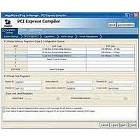
PCI Express Compiler User Guide
Figure 14–1
Related parts for IP-AGX-PCIE/4
Image
Part Number
Description
Manufacturer
Datasheet
Request
R

Part Number:
Description:
IP CORE - X1 Lane PCI Express For Arria GX
Manufacturer:
Altera
Datasheet:

Part Number:
Description:
CYCLONE II STARTER KIT EP2C20N
Manufacturer:
Altera
Datasheet:


Part Number:
Description:
CPLD, EP610 Family, ECMOS Process, 300 Gates, 16 Macro Cells, 16 Reg., 16 User I/Os, 5V Supply, 35 Speed Grade, 24DIP
Manufacturer:
Altera Corporation
Datasheet:
Part Number:
Description:
CPLD, EP610 Family, ECMOS Process, 300 Gates, 16 Macro Cells, 16 Reg., 16 User I/Os, 5V Supply, 15 Speed Grade, 24DIP
Manufacturer:
Altera Corporation
Datasheet:
Part Number:
Description:
Manufacturer:
Altera Corporation
Datasheet:
Part Number:
Description:
CPLD, EP610 Family, ECMOS Process, 300 Gates, 16 Macro Cells, 16 Reg., 16 User I/Os, 5V Supply, 30 Speed Grade, 24DIP
Manufacturer:
Altera Corporation
Datasheet:
Part Number:
Description:
High-performance, low-power erasable programmable logic devices with 8 macrocells, 10ns
Manufacturer:
Altera Corporation
Datasheet:
Part Number:
Description:
High-performance, low-power erasable programmable logic devices with 8 macrocells, 7ns
Manufacturer:
Altera Corporation
Datasheet:
Part Number:
Description:
Classic EPLD
Manufacturer:
Altera Corporation
Datasheet:
Part Number:
Description:
High-performance, low-power erasable programmable logic devices with 8 macrocells, 10ns
Manufacturer:
Altera Corporation
Datasheet:
Part Number:
Description:
Manufacturer:
Altera Corporation
Datasheet:
Part Number:
Description:
Manufacturer:
Altera Corporation
Datasheet:
Part Number:
Description:
Manufacturer:
Altera Corporation
Datasheet: