IP-AGX-PCIE/4 Altera, IP-AGX-PCIE/4 Datasheet - Page 332
IP-AGX-PCIE/4
Manufacturer Part Number
IP-AGX-PCIE/4
Description
IP CORE - PCI Express X1 And X4 Lanes For Arria GX
Manufacturer
Altera
Datasheet
1.IP-AGX-PCIE1.pdf
(362 pages)
Specifications of IP-AGX-PCIE/4
Software Application
IP CORE, Interface And Protocols, PCI
Supported Families
Arria GX, Cyclone II, HardCopy II, Stratix II
Core Architecture
FPGA
Core Sub-architecture
Arria, Cyclone, Stratix
Rohs Compliant
NA
Lead Free Status / RoHS Status
na


B–26
Table B–11. Completion Interface Signals
Incremental Compile Module for Descriptor/Data Examples
PCI Express Compiler User Guide
ko_cpl_spc_vc<n>[19:0]
Notes to
(1) where <n> is 0 - 3 for the ×1 and ×4 cores, and 0 - 1 for the ×8 core
(2) Receive Buffer size consideration: The receive buffer size is variable for the PCIe soft IP variations and fixed to 16 KByte per VC for the hard IP
(1)
variation.The RX Buffer size is set to accommodate optimum throughput of the PCIe link.The receive buffer collects all incoming TLPs from the
PCIe link which consists of posted or non-posted TLPs. When configured as an endpoint, the PCI Express credit advertising mechanism
prevents the RX Buffer from overflowing for all TLP packets except incoming completion TLP packets because the endpoint variation advertises
infinite credits for completion, per the
Therefore for endpoint variations, there could be some rare TLP completion sequences which could lead to a RX Buffer overflow. For example,
a sequence of 3 dword completion TLP using a qword aligned address would require 6 dwords of elapsed time to be written in the RX buffer:
3 dwords for the TLP header, 1 dword for the TLP data, plus 2 dwords of PHY MAC and data link layer overhead. When using the Avalon-ST
128-bit interface, reading this TLP from the RX Buffer requires 8 dwords of elapsed time.Therefore, theoretically, if such completion TLPs are
sent back-to-back, without any gap introduced by DLLP, update FC or a skip character, the RX Buffer will overflow because the read frequency
does not offset the write frequency. This is certainly an extreme case and in practicalities such a sequence has a very low probably of occurring.
However, to ensure that the RX buffer never overflows with completion TLPs, Altera recommended building a circuit in the application layer
which arbitrates the upstream memory read request TLP based on the available space in the completion buffer.
Table
Signal
B–11:
When the descriptor/data PCI Express IP core is generated, the example designs are
generated with an Incremental Compile Module. This module facilitates timing
closure using Quartus II incremental compilation and is provided for backward
compatibility only. The ICM facilitates incremental compilation by providing a fully
registered interface between the user application and the PCI Express transaction
layer. (Refer to
routing of the PCI Express IP core to preserve timing while changes are made to your
application. Altera provides the ICM as clear text to allow its customization if
required.
I/O
O
PCI Express Base Specification Revision 1.1 or
Figure
This static signal reflects the amount of RX buffer space reserved for completion
headers and data. It provides the same information as is shown in the RX buffer
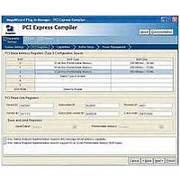
space allocation table of the MegaWizard interface Buffer Setup page (refer to
“Buffer Setup” on page
■
■
The application layer logic is responsible for making sure that the completion
buffer space does not overflow. It needs to limit the number and size of
non-posted requests outstanding to ensure this.
ko_cpl_spc_vc<n>[7:0]: Number of completion headers that can be stored
in the RX buffer.
ko_cpl_spc_vc<n>[19:8]: Number of 16-byte completion data segments
that can be stored in the RX buffer.
B–23) With the ICM, you can lock down the placement and
3–10). The bit field assignments for this signal are:
Incremental Compile Module for Descriptor/Data Examples
Description
2.0.
(2)
December 2010 Altera Corporation
Chapter :
Related parts for IP-AGX-PCIE/4
Image
Part Number
Description
Manufacturer
Datasheet
Request
R

Part Number:
Description:
IP CORE - X1 Lane PCI Express For Arria GX
Manufacturer:
Altera
Datasheet:

Part Number:
Description:
CYCLONE II STARTER KIT EP2C20N
Manufacturer:
Altera
Datasheet:


Part Number:
Description:
CPLD, EP610 Family, ECMOS Process, 300 Gates, 16 Macro Cells, 16 Reg., 16 User I/Os, 5V Supply, 35 Speed Grade, 24DIP
Manufacturer:
Altera Corporation
Datasheet:
Part Number:
Description:
CPLD, EP610 Family, ECMOS Process, 300 Gates, 16 Macro Cells, 16 Reg., 16 User I/Os, 5V Supply, 15 Speed Grade, 24DIP
Manufacturer:
Altera Corporation
Datasheet:
Part Number:
Description:
Manufacturer:
Altera Corporation
Datasheet:
Part Number:
Description:
CPLD, EP610 Family, ECMOS Process, 300 Gates, 16 Macro Cells, 16 Reg., 16 User I/Os, 5V Supply, 30 Speed Grade, 24DIP
Manufacturer:
Altera Corporation
Datasheet:
Part Number:
Description:
High-performance, low-power erasable programmable logic devices with 8 macrocells, 10ns
Manufacturer:
Altera Corporation
Datasheet:
Part Number:
Description:
High-performance, low-power erasable programmable logic devices with 8 macrocells, 7ns
Manufacturer:
Altera Corporation
Datasheet:
Part Number:
Description:
Classic EPLD
Manufacturer:
Altera Corporation
Datasheet:
Part Number:
Description:
High-performance, low-power erasable programmable logic devices with 8 macrocells, 10ns
Manufacturer:
Altera Corporation
Datasheet:
Part Number:
Description:
Manufacturer:
Altera Corporation
Datasheet:
Part Number:
Description:
Manufacturer:
Altera Corporation
Datasheet:
Part Number:
Description:
Manufacturer:
Altera Corporation
Datasheet: