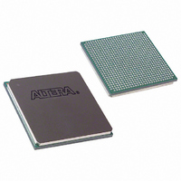
EP1S10F780I6N Altera, EP1S10F780I6N Datasheet - Page 756

EP1S10F780I6N
Manufacturer Part Number
EP1S10F780I6N
Description
IC STRATIX FPGA 10K LE 780-FBGA
Manufacturer
Altera
Series
Stratix®r
Datasheet
1.EP1S10F484I6N.pdf
(864 pages)
Specifications of EP1S10F780I6N
Number Of Logic Elements/cells
10570
Number Of Labs/clbs
1057
Total Ram Bits
920448
Number Of I /o
426
Voltage - Supply
1.425 V ~ 1.575 V
Mounting Type
Surface Mount
Operating Temperature
0°C ~ 85°C
Package / Case
780-FBGA
Lead Free Status / RoHS Status
Lead free / RoHS Compliant
Number Of Gates
-
Available stocks
Company
Part Number
Manufacturer
Quantity
Price
Company:
Part Number:
EP1S10F780I6N
Manufacturer:
ALTERA
Quantity:
3 000
- Current page: 756 of 864
- Download datasheet (11Mb)
Configuration Schemes
11–38
Stratix Device Handbook, Volume 2
During JTAG configuration, data is downloaded to the device on the PCB
through the MasterBlaster or ByteBlasterMV header. Configuring devices
through a cable is similar to programming devices in-system. One
difference is to connect the TRST pin to V
controller is not reset. See
Figure 11–20. JTAG Configuration of a Single Device
Notes to
(1)
(2)
(3)
To configure a single device in a JTAG chain, the programming software
places all other devices in BYPASS mode. In BYPASS mode, devices pass
programming data from the TDI pin to the TDO pin through a single
bypass register without being affected internally. This scheme enables the
programming software to program or verify the target device.
Configuration data driven into the device appears on the TDO pin one
clock cycle later.
V CC
10 kΩ
You should connect the pull-up resistor to the same supply voltage as the
download cable.
You should connect the nCONFIG, MSEL0, and MSEL1 pins to support a non-JTAG
configuration scheme. If you only use JTAG configuration, connect nCONFIG to
V
low.
V
device’s V
this value.
CC
IO
V CC
is a reference voltage for the MasterBlaster output driver. V
, and MSEL0, MSEL1, and MSEL2 to ground. Pull DATA0 and DCLK to high or
Figure
10 kΩ
(2)
(2)
GND
(2)
(2)
(2)
(2)
V CC
CCIO
11–20:
. See the MasterBlaster Serial/USB Communications Cable Data Sheet for
nCE
TRST
nSTATUS
CONF_DONE
nCONFIG
MSEL0
MSEL1
MSEL2
DATA0
DCLK
Stratix GX Device
Stratix or
Figure
TDO
TMS
TCK
TDI
11–20.
1 kΩ
V CC (1)
CC
V CC (1)
to ensure that the TAP
1 kΩ
1 kΩ
GND
MasterBlaster or ByteBlasterMV
Pin 1
Altera Corporation
IO
10-Pin Male Header
should match the
(Top View)
GND
July 2005
V CC (1)
VIO (3)
GND
Related parts for EP1S10F780I6N
Image
Part Number
Description
Manufacturer
Datasheet
Request
R

Part Number:
Description:
CYCLONE II STARTER KIT EP2C20N
Manufacturer:
Altera
Datasheet:

Part Number:
Description:
CPLD, EP610 Family, ECMOS Process, 300 Gates, 16 Macro Cells, 16 Reg., 16 User I/Os, 5V Supply, 35 Speed Grade, 24DIP
Manufacturer:
Altera Corporation
Datasheet:

Part Number:
Description:
CPLD, EP610 Family, ECMOS Process, 300 Gates, 16 Macro Cells, 16 Reg., 16 User I/Os, 5V Supply, 15 Speed Grade, 24DIP
Manufacturer:
Altera Corporation
Datasheet:

Part Number:
Description:
Manufacturer:
Altera Corporation
Datasheet:

Part Number:
Description:
CPLD, EP610 Family, ECMOS Process, 300 Gates, 16 Macro Cells, 16 Reg., 16 User I/Os, 5V Supply, 30 Speed Grade, 24DIP
Manufacturer:
Altera Corporation
Datasheet:

Part Number:
Description:
High-performance, low-power erasable programmable logic devices with 8 macrocells, 10ns
Manufacturer:
Altera Corporation
Datasheet:

Part Number:
Description:
High-performance, low-power erasable programmable logic devices with 8 macrocells, 7ns
Manufacturer:
Altera Corporation
Datasheet:

Part Number:
Description:
Classic EPLD
Manufacturer:
Altera Corporation
Datasheet:

Part Number:
Description:
High-performance, low-power erasable programmable logic devices with 8 macrocells, 10ns
Manufacturer:
Altera Corporation
Datasheet:

Part Number:
Description:
Manufacturer:
Altera Corporation
Datasheet:

Part Number:
Description:
Manufacturer:
Altera Corporation
Datasheet:

Part Number:
Description:
Manufacturer:
Altera Corporation
Datasheet:

Part Number:
Description:
CPLD, EP610 Family, ECMOS Process, 300 Gates, 16 Macro Cells, 16 Reg., 16 User I/Os, 5V Supply, 25 Speed Grade, 24DIP
Manufacturer:
Altera Corporation
Datasheet:


