MPC8379EVRAJF Freescale Semiconductor, MPC8379EVRAJF Datasheet - Page 77
MPC8379EVRAJF
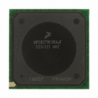
Manufacturer Part Number
MPC8379EVRAJF
Description
MPU PWRQUICC II 533MHZ 689TEPBGA
Manufacturer
Freescale Semiconductor
Series
PowerQUICC II PROr
Datasheets
1.MPC8377EVRAGD.pdf
(126 pages)
2.MPC8377EVRAGD.pdf
(2 pages)
3.MPC8379VRAGD.pdf
(116 pages)
Specifications of MPC8379EVRAJF
Processor Type
MPC83xx PowerQUICC II Pro 32-Bit
Speed
533MHz
Voltage
1V
Mounting Type
Surface Mount
Package / Case
689-TePBGA II
Maximum Clock Frequency
533 MHz
Operating Supply Voltage
1.8 V to 2.5 V
Maximum Operating Temperature
+ 105 C
Mounting Style
SMD/SMT
I/o Voltage
1.8 V, 2.5 V, 3.3 V
Minimum Operating Temperature
0 C
Core Size
32 Bit
Program Memory Size
64KB
Cpu Speed
533MHz
Embedded Interface Type
DUART, HSSI, I2C, IPIC, JTAG, SPI, USB
Digital Ic Case Style
BGA
No. Of Pins
689
Rohs Compliant
Yes
For Use With
MPC8377E-RDBA - BOARD REF DES MPC8377 REV 2.1MPC8377E-MDS-PB - BOARD MODULAR DEV SYSTEM
Lead Free Status / RoHS Status
Lead free / RoHS Compliant
Features
-
Lead Free Status / Rohs Status
Lead free / RoHS Compliant
Available stocks
Company
Part Number
Manufacturer
Quantity
Price
Company:

Part Number:
MPC8379EVRAJF
Manufacturer:
Freescale Semiconductor
Quantity:
135
Company:
Part Number:
MPC8379EVRAJF
Manufacturer:
Freescale Semiconductor
Quantity:
10 000


20.2
Table 70
Figure 48
Figure 49
generally reference the rising edge of the clock, these AC timing diagrams also apply when the falling edge
is the active edge.
Freescale Semiconductor
Output low voltage
Output low voltage
SPI outputs—Master mode (internal clock) delay
SPI outputs—Slave mode (external clock) delay
SPI inputs—Master mode (internal clock) input setup time
SPI inputs—Master mode (internal clock) input hold time
SPI inputs—Slave mode (external clock) input setup time
SPI inputs—Slave mode (external clock) input hold time
Note:
1
2. Output specifications are measured from the 50% level of the rising edge of CLKIN to the 50% level of the signal. Timings
The symbols used for timing specifications follow the pattern of t
inputs and t
timing (NI) for the time SPICLK clock reference (K) goes to the high state (H) until outputs (O) are invalid (X).
are measured at the pin. The maximum SPICLK input frequency is 66.666 MHz.
provides the SPI input and output AC timing specifications.
SPI AC Timing Specifications
provides the AC test load for the SPI.
through
(first two letters of functional block)(reference)(state)(signal)(state)
Parameter
Figure 50
MPC8377E PowerQUICC II Pro Processor Hardware Specifications, Rev. 4
Output
Table 69. SPI DC Electrical Characteristics (continued)
Parameter
represent the AC timing from
Table 70. SPI AC Timing Specifications
Figure 48. SPI AC Test Load
Z
I
0
I
OL
OL
Condition
= 50 Ω
= 3.2 mA
= 8.0 mA
(first two letters of functional block)(signal)(state) (reference)(state)
for outputs. For example, t
Table
Symbol
V
V
OL
OL
R
Symbol
70. Note that although the specifications
t
L
t
t
t
NEKHOV
t
t
NIKHOV
NEIVKH
NEIXKH
NIIVKH
NIIXKH
= 50 Ω
1
Min
—
—
OVDD/2
NIKHOV
Min
0.5
2
4
0
4
2
symbolizes the internal
Max
0.5
0.4
Max
—
—
—
—
6
8
Unit
Unit
ns
ns
ns
ns
ns
ns
V
V
for
SPI
77
Related parts for MPC8379EVRAJF
Image
Part Number
Description
Manufacturer
Datasheet
Request
R

Part Number:
Description:
BOARD REF DESIGN MPC8379E
Manufacturer:
Freescale Semiconductor
Datasheet:

Part Number:
Description:
BOARD REFERENCE FOR MPC837
Manufacturer:
Freescale Semiconductor
Datasheet:
Part Number:
Description:
BOARD PROCESSOR FOR MDS S
Manufacturer:
Freescale Semiconductor
Datasheet:

Part Number:
Description:
Powerquicc Ii Pro Processor Hardware Specifications
Manufacturer:
Freescale Semiconductor, Inc
Datasheet:

Part Number:
Description:
BOARD REF DES MPC8377 REV 2.1
Manufacturer:
Freescale Semiconductor
Datasheet:
Part Number:
Description:
Manufacturer:
Freescale Semiconductor, Inc
Datasheet:
Part Number:
Description:
Manufacturer:
Freescale Semiconductor, Inc
Datasheet:
Part Number:
Description:
Manufacturer:
Freescale Semiconductor, Inc
Datasheet:
Part Number:
Description:
Manufacturer:
Freescale Semiconductor, Inc
Datasheet:
Part Number:
Description:
Manufacturer:
Freescale Semiconductor, Inc
Datasheet:
Part Number:
Description:
Manufacturer:
Freescale Semiconductor, Inc
Datasheet:
Part Number:
Description:
Manufacturer:
Freescale Semiconductor, Inc
Datasheet:
Part Number:
Description:
Manufacturer:
Freescale Semiconductor, Inc
Datasheet:
Part Number:
Description:
Manufacturer:
Freescale Semiconductor, Inc
Datasheet:
Part Number:
Description:
Manufacturer:
Freescale Semiconductor, Inc
Datasheet: