MPC8379EVRAJF Freescale Semiconductor, MPC8379EVRAJF Datasheet - Page 9
MPC8379EVRAJF
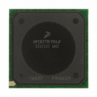
Manufacturer Part Number
MPC8379EVRAJF
Description
MPU PWRQUICC II 533MHZ 689TEPBGA
Manufacturer
Freescale Semiconductor
Series
PowerQUICC II PROr
Datasheets
1.MPC8377EVRAGD.pdf
(126 pages)
2.MPC8377EVRAGD.pdf
(2 pages)
3.MPC8379VRAGD.pdf
(116 pages)
Specifications of MPC8379EVRAJF
Processor Type
MPC83xx PowerQUICC II Pro 32-Bit
Speed
533MHz
Voltage
1V
Mounting Type
Surface Mount
Package / Case
689-TePBGA II
Maximum Clock Frequency
533 MHz
Operating Supply Voltage
1.8 V to 2.5 V
Maximum Operating Temperature
+ 105 C
Mounting Style
SMD/SMT
I/o Voltage
1.8 V, 2.5 V, 3.3 V
Minimum Operating Temperature
0 C
Core Size
32 Bit
Program Memory Size
64KB
Cpu Speed
533MHz
Embedded Interface Type
DUART, HSSI, I2C, IPIC, JTAG, SPI, USB
Digital Ic Case Style
BGA
No. Of Pins
689
Rohs Compliant
Yes
For Use With
MPC8377E-RDBA - BOARD REF DES MPC8377 REV 2.1MPC8377E-MDS-PB - BOARD MODULAR DEV SYSTEM
Lead Free Status / RoHS Status
Lead free / RoHS Compliant
Features
-
Lead Free Status / Rohs Status
Lead free / RoHS Compliant
Available stocks
Company
Part Number
Manufacturer
Quantity
Price
Company:

Part Number:
MPC8379EVRAJF
Manufacturer:
Freescale Semiconductor
Quantity:
135
Company:
Part Number:
MPC8379EVRAJF
Manufacturer:
Freescale Semiconductor
Quantity:
10 000


Figure 2
Freescale Semiconductor
Local Bus
SerDes
Operating temperature range
Notes:
1
2
GV
direction.
L[1,2]_nV
DD
, OV
shows the undershoot and overshoot voltages at the interfaces of the device.
DD
DD
, SDAV
, AV
V
V
Note:
IH
1. Note that t
2. Please note that with the PCI overshoot allowed (as specified above), the device does
not fully comply with the maximum AC ratings and device protection guideline outlined in
the PCI Rev. 2.3 Specification (Section 4.2.2.3).
IL
DD
, and V
DD
G/L/O
MPC8377E PowerQUICC II Pro Processor Hardware Specifications, Rev. 4
G/L/O
_0, XCOREV
Figure 2. Overshoot/Undershoot Voltage for GV
GND – 0.3 V
GND – 0.7 V
Table 3. Recommended Operating Conditions (continued)
DD
Characteristic
VDD
G/L/O
VDD
interface
must track each other and must vary in the same direction—either in the positive or negative
+ 20%
+ 5%
GND
VDD
DD
refers to the clock period associated with the bus clock interface.
, and XPADV
up to 667 MHz
800 MHz
commerical
extended temperature
DD
power inputs.
Not to Exceed 10%
of tinterface1
L[1,2]_nV
Symbol
LBV
T
T
T
T
a
a
j
j
DD
DD
DD
/OV
DD
Recommended
2.5 V ± 125 mV
3.3 V ± 165 mV
1.05 V ± 50 mV
T
1.8 V ± 90 mV
T
T
T
a
1.0 ± 50 mV
/LV
=–40 (min)—
a
j
j
=125 (max)
=125 (max)
=0 (min)—
Value
DD
Electrical Characteristics
Unit
°C
°C
V
V
V
Notes
1, 2
1, 2
—
—
—
9
Related parts for MPC8379EVRAJF
Image
Part Number
Description
Manufacturer
Datasheet
Request
R

Part Number:
Description:
BOARD REF DESIGN MPC8379E
Manufacturer:
Freescale Semiconductor
Datasheet:

Part Number:
Description:
BOARD REFERENCE FOR MPC837
Manufacturer:
Freescale Semiconductor
Datasheet:
Part Number:
Description:
BOARD PROCESSOR FOR MDS S
Manufacturer:
Freescale Semiconductor
Datasheet:

Part Number:
Description:
Powerquicc Ii Pro Processor Hardware Specifications
Manufacturer:
Freescale Semiconductor, Inc
Datasheet:

Part Number:
Description:
BOARD REF DES MPC8377 REV 2.1
Manufacturer:
Freescale Semiconductor
Datasheet:
Part Number:
Description:
Manufacturer:
Freescale Semiconductor, Inc
Datasheet:
Part Number:
Description:
Manufacturer:
Freescale Semiconductor, Inc
Datasheet:
Part Number:
Description:
Manufacturer:
Freescale Semiconductor, Inc
Datasheet:
Part Number:
Description:
Manufacturer:
Freescale Semiconductor, Inc
Datasheet:
Part Number:
Description:
Manufacturer:
Freescale Semiconductor, Inc
Datasheet:
Part Number:
Description:
Manufacturer:
Freescale Semiconductor, Inc
Datasheet:
Part Number:
Description:
Manufacturer:
Freescale Semiconductor, Inc
Datasheet:
Part Number:
Description:
Manufacturer:
Freescale Semiconductor, Inc
Datasheet:
Part Number:
Description:
Manufacturer:
Freescale Semiconductor, Inc
Datasheet:
Part Number:
Description:
Manufacturer:
Freescale Semiconductor, Inc
Datasheet: