MPC8379EVRAJF Freescale Semiconductor, MPC8379EVRAJF Datasheet - Page 17
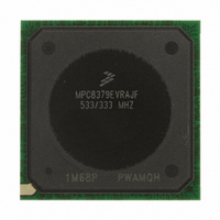
MPC8379EVRAJF
Manufacturer Part Number
MPC8379EVRAJF
Description
MPU PWRQUICC II 533MHZ 689TEPBGA
Manufacturer
Freescale Semiconductor
Series
PowerQUICC II PROr
Datasheets
1.MPC8377EVRAGD.pdf
(126 pages)
2.MPC8377EVRAGD.pdf
(2 pages)
3.MPC8379VRAGD.pdf
(116 pages)
Specifications of MPC8379EVRAJF
Processor Type
MPC83xx PowerQUICC II Pro 32-Bit
Speed
533MHz
Voltage
1V
Mounting Type
Surface Mount
Package / Case
689-TePBGA II
Maximum Clock Frequency
533 MHz
Operating Supply Voltage
1.8 V to 2.5 V
Maximum Operating Temperature
+ 105 C
Mounting Style
SMD/SMT
I/o Voltage
1.8 V, 2.5 V, 3.3 V
Minimum Operating Temperature
0 C
Core Size
32 Bit
Program Memory Size
64KB
Cpu Speed
533MHz
Embedded Interface Type
DUART, HSSI, I2C, IPIC, JTAG, SPI, USB
Digital Ic Case Style
BGA
No. Of Pins
689
Rohs Compliant
Yes
For Use With
MPC8377E-RDBA - BOARD REF DES MPC8377 REV 2.1MPC8377E-MDS-PB - BOARD MODULAR DEV SYSTEM
Lead Free Status / RoHS Status
Lead free / RoHS Compliant
Features
-
Lead Free Status / Rohs Status
Lead free / RoHS Compliant
Available stocks
Company
Part Number
Manufacturer
Quantity
Price
Company:

Part Number:
MPC8379EVRAJF
Manufacturer:
Freescale Semiconductor
Quantity:
135
Company:
Part Number:
MPC8379EVRAJF
Manufacturer:
Freescale Semiconductor
Quantity:
10 000


Table 14
Table 15
GV
Freescale Semiconductor
Output low current (V
Note:
1
2
3
4
5
Input/output capacitance: DQ, DQS, DQS
Delta input/output capacitance: DQ, DQS, DQS
Note:
1
I/O supply voltage
I/O reference voltage
I/O termination voltage
Input high voltage
Input low voltage
Output leakage current
Output high current (V
Output low current (V
Note:
1
2
3
4
5
GV
MV
noise on MV
V
equal to MV
Output leakage is measured with all outputs disabled, 0 V
See AN3665, “MPC837xE Design Checklist,” for proper DDR termination.
This parameter is sampled. GV
GV
MV
noise on MV
V
equal to MV
Output leakage is measured with all outputs disabled, 0 V
See AN3665, “MPC837xE Design Checklist,” for proper DDR termination.
DD
TT
TT
DD
REF
DD
REF
is not applied directly to the device. It is the supply to which far end signal termination is made and is expected to be
is not applied directly to the device. It is the supply to which far end signal termination is made and is expected to be
(typ) = 2.5 V
is expected to be within 50 mV of the DRAM GV
is expected to be within 50 mV of the DRAM GV
is expected to be equal to 0.5 × GV
is expected to be equal to 0.5 × GV
provides the DDR2 capacitance when GV
provides the recommended operating conditions for the DDR SDRAM component(s) when
Table 13. DDR2 SDRAM DC Electrical Characteristics for GV
REF
REF
REF
REF
Parameter
Parameter
. This rail should track variations in the DC level of MV
. This rail should track variations in the DC level of MV
Table 15. DDR SDRAM DC Electrical Characteristics for GV
may not exceed ±2% of the DC value.
may not exceed ±2% of the DC value.
Parameter
OUT
OUT
OUT
.
MPC8377E PowerQUICC II Pro Processor Hardware Specifications, Rev. 4
= 0.3 V)
= 0.38 V)
= 1.9 V)
Table 14. DDR2 SDRAM Capacitance for GV
DD
= 1.8 V ± 0.090 V, f = 1 MHz, T
DD
DD
, and to track GV
, and to track GV
Symbol
Symbol
MV
GV
V
I
V
I
V
I
I
OH
OL
OZ
OL
TT
IH
REF
IL
DD
Symbol
DD
DD
C
C
DIO
IO
at all times.
at all times.
≤
≤
DD
V
V
OUT
OUT
(typ) = 1.8 V.
MV
MV
DD
DD
0.49 × GV
A
DC variations as measured at the receiver. Peak-to-peak
REF
REF
DC variations as measured at the receiver. Peak-to-peak
13.4
Min
≤
≤
2.375
–15.2
= 25°C, V
–0.3
15.2
Min
–40
GV
GV
REF
REF
+ 0.18
– 0.04
DD
DD
Min
.
.
—
DD
6
.
.
OUT
DD
DD
(typ) = 1.8 V
= GV
(typ) = 1.8 V (continued)
MV
MV
0.51 × GV
GV
DD
DD
REF
REF
Max
2.625
DD
—
Max
Max
/2, V
0.5
40
—
—
(typ) = 2.5 V
8
+ 0.04
+ 0.3
– 0.18
OUT
DD
(peak-to-peak) = 0.2 V.
DDR1 and DDR2 SDRAM
Unit
pF
pF
Unit
Unit
mA
mA
mA
μA
V
V
V
V
V
Notes
Notes
Notes
2, 5
—
1
1
—
—
—
—
1
3
4
17
Related parts for MPC8379EVRAJF
Image
Part Number
Description
Manufacturer
Datasheet
Request
R

Part Number:
Description:
BOARD REF DESIGN MPC8379E
Manufacturer:
Freescale Semiconductor
Datasheet:

Part Number:
Description:
BOARD REFERENCE FOR MPC837
Manufacturer:
Freescale Semiconductor
Datasheet:
Part Number:
Description:
BOARD PROCESSOR FOR MDS S
Manufacturer:
Freescale Semiconductor
Datasheet:

Part Number:
Description:
Powerquicc Ii Pro Processor Hardware Specifications
Manufacturer:
Freescale Semiconductor, Inc
Datasheet:

Part Number:
Description:
BOARD REF DES MPC8377 REV 2.1
Manufacturer:
Freescale Semiconductor
Datasheet:
Part Number:
Description:
Manufacturer:
Freescale Semiconductor, Inc
Datasheet:
Part Number:
Description:
Manufacturer:
Freescale Semiconductor, Inc
Datasheet:
Part Number:
Description:
Manufacturer:
Freescale Semiconductor, Inc
Datasheet:
Part Number:
Description:
Manufacturer:
Freescale Semiconductor, Inc
Datasheet:
Part Number:
Description:
Manufacturer:
Freescale Semiconductor, Inc
Datasheet:
Part Number:
Description:
Manufacturer:
Freescale Semiconductor, Inc
Datasheet:
Part Number:
Description:
Manufacturer:
Freescale Semiconductor, Inc
Datasheet:
Part Number:
Description:
Manufacturer:
Freescale Semiconductor, Inc
Datasheet:
Part Number:
Description:
Manufacturer:
Freescale Semiconductor, Inc
Datasheet:
Part Number:
Description:
Manufacturer:
Freescale Semiconductor, Inc
Datasheet: