MPC8379EVRAJF Freescale Semiconductor, MPC8379EVRAJF Datasheet - Page 16
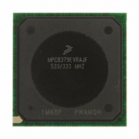
MPC8379EVRAJF
Manufacturer Part Number
MPC8379EVRAJF
Description
MPU PWRQUICC II 533MHZ 689TEPBGA
Manufacturer
Freescale Semiconductor
Series
PowerQUICC II PROr
Datasheets
1.MPC8377EVRAGD.pdf
(126 pages)
2.MPC8377EVRAGD.pdf
(2 pages)
3.MPC8379VRAGD.pdf
(116 pages)
Specifications of MPC8379EVRAJF
Processor Type
MPC83xx PowerQUICC II Pro 32-Bit
Speed
533MHz
Voltage
1V
Mounting Type
Surface Mount
Package / Case
689-TePBGA II
Maximum Clock Frequency
533 MHz
Operating Supply Voltage
1.8 V to 2.5 V
Maximum Operating Temperature
+ 105 C
Mounting Style
SMD/SMT
I/o Voltage
1.8 V, 2.5 V, 3.3 V
Minimum Operating Temperature
0 C
Core Size
32 Bit
Program Memory Size
64KB
Cpu Speed
533MHz
Embedded Interface Type
DUART, HSSI, I2C, IPIC, JTAG, SPI, USB
Digital Ic Case Style
BGA
No. Of Pins
689
Rohs Compliant
Yes
For Use With
MPC8377E-RDBA - BOARD REF DES MPC8377 REV 2.1MPC8377E-MDS-PB - BOARD MODULAR DEV SYSTEM
Lead Free Status / RoHS Status
Lead free / RoHS Compliant
Features
-
Lead Free Status / Rohs Status
Lead free / RoHS Compliant
Available stocks
Company
Part Number
Manufacturer
Quantity
Price
Company:

Part Number:
MPC8379EVRAJF
Manufacturer:
Freescale Semiconductor
Quantity:
135
Company:
Part Number:
MPC8379EVRAJF
Manufacturer:
Freescale Semiconductor
Quantity:
10 000


DDR1 and DDR2 SDRAM
Table 12
6
This section describes the DC and AC electrical specifications for the DDR SDRAM interface of the
MPC8377E. Note that DDR1 SDRAM is GV
6.1
Table 13
device when GV
16
Time for the device to turn off POR config signals with respect to the assertion of
HRESET
Time for the device to start driving functional output signals multiplexed with the
POR configuration signals with respect to the negation of HRESET
Note:
1
2
3
I/O supply voltage
I/O reference voltage
I/O termination voltage
Input high voltage
Input low voltage
Output leakage current
Output high current (V
PLL lock times
Note:
• The device guarantees the PLL lock if the clock settings are within spec range. The core clock also depends on the core PLL
t
clock is applied to the CLKIN input, and PCI_SYNC_IN period depends on the value of CFG_CLKIN_DIV. See the MPC8379E
Integrated Host Processor Reference Manual for more details.
t
MPC8379E Integrated Host Processor Reference Manual for more details.
POR config signals consists of CFG_RESET_SOURCE[0:3], CFG_LBMUX, and CFG_CLKIN_DIV.
PCI_SYNC_IN
CLKIN
ratio. See
DDR1 and DDR2 SDRAM
is the clock period of the input clock applied to CLKIN. It is only valid when the device is in PCI host mode. See the
provides the PLL lock times.
provides the recommended operating conditions for the DDR2 SDRAM component(s) of the
DDR1 and DDR2 SDRAM DC Electrical Characteristics
Section 23, “Clocking,”
is the clock period of the input clock applied to PCI_SYNC_IN. When the device is In PCI host mode the primary
Parameter
Parameter
Table 13. DDR2 SDRAM DC Electrical Characteristics for GV
DD
OUT
(typ) = 1.8 V
MPC8377E PowerQUICC II Pro Processor Hardware Specifications, Rev. 4
Table 11. RESET Initialization Timing Specifications (continued)
= 1.40 V)
Parameter/Condition
for more information.
.
Table 12. PLL Lock Times
Symbol
MV
GV
V
I
V
I
V
OZ
OH
TT
REF
IH
IL
DD
DD
Min
—
(typ) = 2.5 V and DDR2 SDRAM is GV
MV
MV
0.49 × GV
REF
REF
–13.4
1.71
–0.3
Min
–40
+ 0.140
– 0.04
DD
Max
100
Min
MV
—
MV
1
0.51 × GV
GV
REF
REF
DD
Max
1.89
DD
40
—
– 0.140
+ 0.04
(typ) = 1.8 V
+ 0.3
Max
—
4
DD
Unit
μs
Freescale Semiconductor
t
PCI_SYNC_IN
DD
Unit
Unit
ns
mA
μA
V
V
V
V
V
(typ) = 1.8 V.
Notes
Notes
—
Notes
2, 5
—
—
—
1, 3
1
3
4
3
Related parts for MPC8379EVRAJF
Image
Part Number
Description
Manufacturer
Datasheet
Request
R

Part Number:
Description:
BOARD REF DESIGN MPC8379E
Manufacturer:
Freescale Semiconductor
Datasheet:

Part Number:
Description:
BOARD REFERENCE FOR MPC837
Manufacturer:
Freescale Semiconductor
Datasheet:
Part Number:
Description:
BOARD PROCESSOR FOR MDS S
Manufacturer:
Freescale Semiconductor
Datasheet:

Part Number:
Description:
Powerquicc Ii Pro Processor Hardware Specifications
Manufacturer:
Freescale Semiconductor, Inc
Datasheet:

Part Number:
Description:
BOARD REF DES MPC8377 REV 2.1
Manufacturer:
Freescale Semiconductor
Datasheet:
Part Number:
Description:
Manufacturer:
Freescale Semiconductor, Inc
Datasheet:
Part Number:
Description:
Manufacturer:
Freescale Semiconductor, Inc
Datasheet:
Part Number:
Description:
Manufacturer:
Freescale Semiconductor, Inc
Datasheet:
Part Number:
Description:
Manufacturer:
Freescale Semiconductor, Inc
Datasheet:
Part Number:
Description:
Manufacturer:
Freescale Semiconductor, Inc
Datasheet:
Part Number:
Description:
Manufacturer:
Freescale Semiconductor, Inc
Datasheet:
Part Number:
Description:
Manufacturer:
Freescale Semiconductor, Inc
Datasheet:
Part Number:
Description:
Manufacturer:
Freescale Semiconductor, Inc
Datasheet:
Part Number:
Description:
Manufacturer:
Freescale Semiconductor, Inc
Datasheet:
Part Number:
Description:
Manufacturer:
Freescale Semiconductor, Inc
Datasheet: