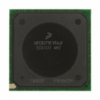
MPC8379EVRAJF Freescale Semiconductor, MPC8379EVRAJF Datasheet - Page 81

MPC8379EVRAJF
Manufacturer Part Number
MPC8379EVRAJF
Description
MPU PWRQUICC II 533MHZ 689TEPBGA
Manufacturer
Freescale Semiconductor
Series
PowerQUICC II PROr
Datasheets
1.MPC8377EVRAGD.pdf
(126 pages)
2.MPC8377EVRAGD.pdf
(2 pages)
3.MPC8379VRAGD.pdf
(116 pages)
Specifications of MPC8379EVRAJF
Processor Type
MPC83xx PowerQUICC II Pro 32-Bit
Speed
533MHz
Voltage
1V
Mounting Type
Surface Mount
Package / Case
689-TePBGA II
Maximum Clock Frequency
533 MHz
Operating Supply Voltage
1.8 V to 2.5 V
Maximum Operating Temperature
+ 105 C
Mounting Style
SMD/SMT
I/o Voltage
1.8 V, 2.5 V, 3.3 V
Minimum Operating Temperature
0 C
Core Size
32 Bit
Program Memory Size
64KB
Cpu Speed
533MHz
Embedded Interface Type
DUART, HSSI, I2C, IPIC, JTAG, SPI, USB
Digital Ic Case Style
BGA
No. Of Pins
689
Rohs Compliant
Yes
For Use With
MPC8377E-RDBA - BOARD REF DES MPC8377 REV 2.1MPC8377E-MDS-PB - BOARD MODULAR DEV SYSTEM
Lead Free Status / RoHS Status
Lead free / RoHS Compliant
Features
-
Lead Free Status / Rohs Status
Lead free / RoHS Compliant
Available stocks
Company
Part Number
Manufacturer
Quantity
Price
Company:
Part Number:
MPC8379EVRAJF
Manufacturer:
Freescale Semiconductor
Quantity:
135
Company:
Part Number:
MPC8379EVRAJF
Manufacturer:
Freescale Semiconductor
Quantity:
10 000
21.2.2
The DC level requirement for the device SerDes reference clock inputs is different depending on the
signaling mode used to connect the clock driver chip and SerDes reference clock inputs as described
below.
Freescale Semiconductor
•
•
•
— The SerDes reference clock input can be either differential or single-ended. Refer to the
The maximum average current requirement that also determines the common mode voltage range
— When the SerDes reference clock differential inputs are DC coupled externally with the clock
— This current limitation sets the maximum common mode input voltage to be less than 0.4 V
— If the device driving the SDn_REF_CLK and SDn_REF_CLK inputs cannot drive 50 Ω to
The input amplitude requirement
— This requirement is described in detail in the following sections.
Differential Mode
— The input amplitude of the differential clock must be between 400 mV and 1600 mV
Differential Mode and Single-ended Mode description below for further detailed requirements.
driver chip, the maximum average current allowed for each input pin is 8 mA. In this case, the
exact common mode input voltage is not critical as long as it is within the range allowed by the
maximum average current of 8 mA (refer to the following bullet for more detail), since the
input is AC-coupled on-chip.
(0.4 V ÷ 50 = 8 mA) while the minimum common mode input level is 0.1 V above
SGND_SRDSn (xcorevss). For example, a clock with a 50/50 duty cycle can be produced by
a clock driver with output driven by its current source from 0 mA to 16 mA (0–0.8 V), such
that each phase of the differential input has a single-ended swing from 0 V to 800 mV with the
common mode voltage at 400 mV.
SGND_SRDSn (xcorevss) DC, or it exceeds the maximum input current limitations, then it
must be AC-coupled off-chip.
differential peak-peak (or between 200 mV and 800 mV differential peak). In other words,
each signal wire of the differential pair must have a single-ended swing less than 800 mV and
DC Level Requirement for SerDes Reference Clocks
MPC8377E PowerQUICC II Pro Processor Hardware Specifications, Rev. 4
SDn_REF_CLK
SDn_REF_CLK
Figure 52. Receiver of SerDes Reference Clocks
50 Ω
50 Ω
Input
Amp
High-Speed Serial Interfaces (HSSI)
81


