MPC8379EVRAJF Freescale Semiconductor, MPC8379EVRAJF Datasheet - Page 69
MPC8379EVRAJF
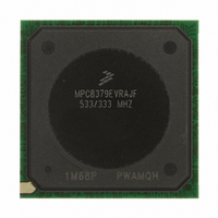
Manufacturer Part Number
MPC8379EVRAJF
Description
MPU PWRQUICC II 533MHZ 689TEPBGA
Manufacturer
Freescale Semiconductor
Series
PowerQUICC II PROr
Datasheets
1.MPC8377EVRAGD.pdf
(126 pages)
2.MPC8377EVRAGD.pdf
(2 pages)
3.MPC8379VRAGD.pdf
(116 pages)
Specifications of MPC8379EVRAJF
Processor Type
MPC83xx PowerQUICC II Pro 32-Bit
Speed
533MHz
Voltage
1V
Mounting Type
Surface Mount
Package / Case
689-TePBGA II
Maximum Clock Frequency
533 MHz
Operating Supply Voltage
1.8 V to 2.5 V
Maximum Operating Temperature
+ 105 C
Mounting Style
SMD/SMT
I/o Voltage
1.8 V, 2.5 V, 3.3 V
Minimum Operating Temperature
0 C
Core Size
32 Bit
Program Memory Size
64KB
Cpu Speed
533MHz
Embedded Interface Type
DUART, HSSI, I2C, IPIC, JTAG, SPI, USB
Digital Ic Case Style
BGA
No. Of Pins
689
Rohs Compliant
Yes
For Use With
MPC8377E-RDBA - BOARD REF DES MPC8377 REV 2.1MPC8377E-MDS-PB - BOARD MODULAR DEV SYSTEM
Lead Free Status / RoHS Status
Lead free / RoHS Compliant
Features
-
Lead Free Status / Rohs Status
Lead free / RoHS Compliant
Available stocks
Company
Part Number
Manufacturer
Quantity
Price
Company:

Part Number:
MPC8379EVRAJF
Manufacturer:
Freescale Semiconductor
Quantity:
135
Company:
Part Number:
MPC8379EVRAJF
Manufacturer:
Freescale Semiconductor
Quantity:
10 000


15.5.1
The AC timing and voltage parameters must be verified at the measurement point, as specified within
0.2 inches of the package pins, into a test/measurement load shown in
16 Serial ATA (SATA)
This section describes the DC and AC electrical specifications for the serial ATA (SATA) of the
MPC8377E. Note that the external cabled applications or long backplane applications (Gen1x and Gen2x)
are not supported.
16.1
The reference clock is a single ended input clock required for the SATA interface operation. The AC
requirements for the SATA reference clock are listed in the
Freescale Semiconductor
SD_REF_CLK/ SD_REF_CLK
frequency range
SD_REF_CLK/ SD_REF_CLK
clock frequency tolerance
SD_REF_CLK/ SD_REF_CLK
reference clock duty cycle
Requirements for SATA REF_CLK
Parameter
Compliance Test and Measurement Load
The allowance of the measurement point to be within 0.2 inches of the
package pins is meant to acknowledge that package/board routing may
benefit from D+ and D– not being exactly matched in length at the package
pin boundary. If the vendor does not explicitly state where the measurement
point is located, the measurement point is assumed to be the D+ and D–
package pins.
MPC8377E PowerQUICC II Pro Processor Hardware Specifications, Rev. 4
D+ Package Pin
D– Package Pin
Table 54. SATA Reference Clock Input Requirements
TX Silicon +
Figure 44. Compliance Test/Measurement Load
Package
Measured at 1.6V
Condition
—
—
NOTE
t
t
CLK_DUTY
t
Symbol
CLK_REF
CLK_TOL
R = 50 Ω
C = C
C = C
TX
TX
Table
–350
Min
40
—
54.
100/125/150
Figure
R = 50 Ω
Typical
50
0
44.
+350
Max
—
60
Serial ATA (SATA)
MHz
Unit
ppm
%
Notes
—
—
1
69
Related parts for MPC8379EVRAJF
Image
Part Number
Description
Manufacturer
Datasheet
Request
R

Part Number:
Description:
BOARD REF DESIGN MPC8379E
Manufacturer:
Freescale Semiconductor
Datasheet:

Part Number:
Description:
BOARD REFERENCE FOR MPC837
Manufacturer:
Freescale Semiconductor
Datasheet:
Part Number:
Description:
BOARD PROCESSOR FOR MDS S
Manufacturer:
Freescale Semiconductor
Datasheet:

Part Number:
Description:
Powerquicc Ii Pro Processor Hardware Specifications
Manufacturer:
Freescale Semiconductor, Inc
Datasheet:

Part Number:
Description:
BOARD REF DES MPC8377 REV 2.1
Manufacturer:
Freescale Semiconductor
Datasheet:
Part Number:
Description:
Manufacturer:
Freescale Semiconductor, Inc
Datasheet:
Part Number:
Description:
Manufacturer:
Freescale Semiconductor, Inc
Datasheet:
Part Number:
Description:
Manufacturer:
Freescale Semiconductor, Inc
Datasheet:
Part Number:
Description:
Manufacturer:
Freescale Semiconductor, Inc
Datasheet:
Part Number:
Description:
Manufacturer:
Freescale Semiconductor, Inc
Datasheet:
Part Number:
Description:
Manufacturer:
Freescale Semiconductor, Inc
Datasheet:
Part Number:
Description:
Manufacturer:
Freescale Semiconductor, Inc
Datasheet:
Part Number:
Description:
Manufacturer:
Freescale Semiconductor, Inc
Datasheet:
Part Number:
Description:
Manufacturer:
Freescale Semiconductor, Inc
Datasheet:
Part Number:
Description:
Manufacturer:
Freescale Semiconductor, Inc
Datasheet: