MPC8379EVRAJF Freescale Semiconductor, MPC8379EVRAJF Datasheet - Page 26
MPC8379EVRAJF
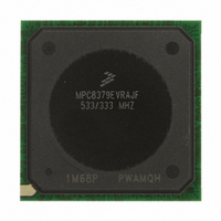
Manufacturer Part Number
MPC8379EVRAJF
Description
MPU PWRQUICC II 533MHZ 689TEPBGA
Manufacturer
Freescale Semiconductor
Series
PowerQUICC II PROr
Datasheets
1.MPC8377EVRAGD.pdf
(126 pages)
2.MPC8377EVRAGD.pdf
(2 pages)
3.MPC8379VRAGD.pdf
(116 pages)
Specifications of MPC8379EVRAJF
Processor Type
MPC83xx PowerQUICC II Pro 32-Bit
Speed
533MHz
Voltage
1V
Mounting Type
Surface Mount
Package / Case
689-TePBGA II
Maximum Clock Frequency
533 MHz
Operating Supply Voltage
1.8 V to 2.5 V
Maximum Operating Temperature
+ 105 C
Mounting Style
SMD/SMT
I/o Voltage
1.8 V, 2.5 V, 3.3 V
Minimum Operating Temperature
0 C
Core Size
32 Bit
Program Memory Size
64KB
Cpu Speed
533MHz
Embedded Interface Type
DUART, HSSI, I2C, IPIC, JTAG, SPI, USB
Digital Ic Case Style
BGA
No. Of Pins
689
Rohs Compliant
Yes
For Use With
MPC8377E-RDBA - BOARD REF DES MPC8377 REV 2.1MPC8377E-MDS-PB - BOARD MODULAR DEV SYSTEM
Lead Free Status / RoHS Status
Lead free / RoHS Compliant
Features
-
Lead Free Status / Rohs Status
Lead free / RoHS Compliant
Available stocks
Company
Part Number
Manufacturer
Quantity
Price
Company:

Part Number:
MPC8379EVRAJF
Manufacturer:
Freescale Semiconductor
Quantity:
135
Company:
Part Number:
MPC8379EVRAJF
Manufacturer:
Freescale Semiconductor
Quantity:
10 000


Ethernet: Enhanced Three-Speed Ethernet (eTSEC)
Figure 8
Figure 9
8.2.2
Table 28
26
At recommended operating conditions with LV
At recommended operating conditions with LV
RX_CLK clock rise time (20%–80%)
RX_CLK clock fall time (80%–20%)
1. The symbols used for timing specifications herein follow the pattern of t
Data to clock output skew (at transmitter)
Data to clock input skew (at receiver)
Clock period
for inputs and t
receive timing (MR) with respect to the time data input signals (D) reach the valid state (V) relative to the t
(K) going to the high (H) state or setup time. Also, t
input signals (D) went invalid (X) relative to the t
general, the clock reference symbol representation is based on three letters representing the clock of a particular functional.
For example, the subscript of t
used with the appropriate letter: R (rise) or F (fall).
provides the AC test load for eTSEC.
shows the MII receive AC timing diagram.
presents the RGMII and RTBI AC timing specifications.
RGMII and RTBI AC Timing
(first two letters of functional block)(reference)(state)(signal)(state)
Parameter
RXD[3:0]
RX_CLK
RX_ER
RX_DV
Parameter
MPC8377E PowerQUICC II Pro Processor Hardware Specifications, Rev. 4
Output
Table 27. MII Receive AC Timing Specifications (continued)
Table 28. RGMII and RTBI AC Timing Specifications
MRX
represents the MII (M) receive (RX) clock. For rise and fall times, the latter convention is
t
Figure 9. MII Receive AC Timing Diagram
t
MRXH
MRDVKH
DD
DD
of 3.3 V ± 5%.
of 2.5 V ± 5%.
Figure 8. eTSEC AC Test Load
t
MRX
Z
0
MRX
= 50 Ω
Symbol
MRDXKL
t
t
SKRGT
SKRGT
clock reference (K) going to the low (L) state or hold time. Note that, in
t
RGT
Valid Data
Symbol
t
t
MRXR
Specifications
MRXF
1
symbolizes MII receive timing (GR) with respect to the time data
t
MRXF
1
–600
Min
for outputs. For example, t
1.0
7.2
(first two letters of functional block)(signal)(state) (reference)(state)
R
t
Min
MRDXKL
1.0
1.0
t
L
MRXR
= 50 Ω
Typical
8.0
—
0
Typical
LVDD/2
—
—
MRDVKH
Max
600
2.8
8.8
Freescale Semiconductor
Max
4.0
4.0
symbolizes MII
MRX
Unit
clock reference
ps
ns
ns
Notes
Unit
ns
ns
—
2
3
Related parts for MPC8379EVRAJF
Image
Part Number
Description
Manufacturer
Datasheet
Request
R

Part Number:
Description:
BOARD REF DESIGN MPC8379E
Manufacturer:
Freescale Semiconductor
Datasheet:

Part Number:
Description:
BOARD REFERENCE FOR MPC837
Manufacturer:
Freescale Semiconductor
Datasheet:
Part Number:
Description:
BOARD PROCESSOR FOR MDS S
Manufacturer:
Freescale Semiconductor
Datasheet:

Part Number:
Description:
Powerquicc Ii Pro Processor Hardware Specifications
Manufacturer:
Freescale Semiconductor, Inc
Datasheet:

Part Number:
Description:
BOARD REF DES MPC8377 REV 2.1
Manufacturer:
Freescale Semiconductor
Datasheet:
Part Number:
Description:
Manufacturer:
Freescale Semiconductor, Inc
Datasheet:
Part Number:
Description:
Manufacturer:
Freescale Semiconductor, Inc
Datasheet:
Part Number:
Description:
Manufacturer:
Freescale Semiconductor, Inc
Datasheet:
Part Number:
Description:
Manufacturer:
Freescale Semiconductor, Inc
Datasheet:
Part Number:
Description:
Manufacturer:
Freescale Semiconductor, Inc
Datasheet:
Part Number:
Description:
Manufacturer:
Freescale Semiconductor, Inc
Datasheet:
Part Number:
Description:
Manufacturer:
Freescale Semiconductor, Inc
Datasheet:
Part Number:
Description:
Manufacturer:
Freescale Semiconductor, Inc
Datasheet:
Part Number:
Description:
Manufacturer:
Freescale Semiconductor, Inc
Datasheet:
Part Number:
Description:
Manufacturer:
Freescale Semiconductor, Inc
Datasheet: