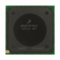
MPC8379EVRAJF Freescale Semiconductor, MPC8379EVRAJF Datasheet - Page 51

MPC8379EVRAJF
Manufacturer Part Number
MPC8379EVRAJF
Description
MPU PWRQUICC II 533MHZ 689TEPBGA
Manufacturer
Freescale Semiconductor
Series
PowerQUICC II PROr
Datasheets
1.MPC8377EVRAGD.pdf
(126 pages)
2.MPC8377EVRAGD.pdf
(2 pages)
3.MPC8379VRAGD.pdf
(116 pages)
Specifications of MPC8379EVRAJF
Processor Type
MPC83xx PowerQUICC II Pro 32-Bit
Speed
533MHz
Voltage
1V
Mounting Type
Surface Mount
Package / Case
689-TePBGA II
Maximum Clock Frequency
533 MHz
Operating Supply Voltage
1.8 V to 2.5 V
Maximum Operating Temperature
+ 105 C
Mounting Style
SMD/SMT
I/o Voltage
1.8 V, 2.5 V, 3.3 V
Minimum Operating Temperature
0 C
Core Size
32 Bit
Program Memory Size
64KB
Cpu Speed
533MHz
Embedded Interface Type
DUART, HSSI, I2C, IPIC, JTAG, SPI, USB
Digital Ic Case Style
BGA
No. Of Pins
689
Rohs Compliant
Yes
For Use With
MPC8377E-RDBA - BOARD REF DES MPC8377 REV 2.1MPC8377E-MDS-PB - BOARD MODULAR DEV SYSTEM
Lead Free Status / RoHS Status
Lead free / RoHS Compliant
Features
-
Lead Free Status / Rohs Status
Lead free / RoHS Compliant
Available stocks
Company
Part Number
Manufacturer
Quantity
Price
Company:
Part Number:
MPC8379EVRAJF
Manufacturer:
Freescale Semiconductor
Quantity:
135
Company:
Part Number:
MPC8379EVRAJF
Manufacturer:
Freescale Semiconductor
Quantity:
10 000
11.3.1.2
The following equations show how to calculate the allowed skew range between the SD_CLK and
SD_DAT/CMD signals on the PCB.
This means that clock can be delayed versus data up to 8 ns (external delay line) in ideal case of
t
11.3.2
Figure 31
For the input path, the device eSDHC expects to sample the data 1.5 internal clock cycles after it was
driven by the SD card. Since in this mode the SD card drives the data at the rising edge of the clock, a
sufficient delay to the clock and the data must exist to ensure it will not be sampled at the wrong internal
clock falling edge. Note that the internal clock which is guaranteed to be 50% duty cycle is used to sample
the data, and therefore used in the equations.
Freescale Semiconductor
SHSCLKL
t
t
MPC8377E Pins
CLK_DELAY
CLK_DELAY
Output from the
MPC8377E Pin
SD CLK at the
SD Card Pins
= 10 ns:
provides the data and command input timing diagram.
the Card Pin
High-Speed Input Path (Read)
Input at the
SD CLK at
High-Speed Write Meeting Hold (Minimum Delay)
MPC8377E PowerQUICC II Pro Processor Hardware Specifications, Rev. 4
–
–
t
t
DATA_DELAY
DATA_DELAY
t
t
CLK_DELAY
CLK_DELAY
Driving
Edge
t
1/2 Cycle
ODLY
t
OH
t
< t
–
SHSCK
< 10 + 0
< 8
Figure 31. High-Speed Input Path
t
DATA_DELAY
SHSCKL
t
CLK_DELAY
(Clock Cycle)
+ t
–
Wrong Edge
2
(MPC8377E Input Setup)
SHSKHOX
< t
SHSCKL
t
DATA_DELAY
+ t
+ t
DATA_DELAY
t
SHSKHOX
SHSIVKH
Enhanced Secure Digital Host Controller (eSDHC)
–
–
t
t
IH
IH
Right Edge
Sampling
Edge
(MPC8377E Input Hold)
t
SHSIXKH
Eqn. 13
Eqn. 14
51


