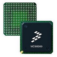
MC68360CAI25L Freescale Semiconductor, MC68360CAI25L Datasheet - Page 298

MC68360CAI25L
Manufacturer Part Number
MC68360CAI25L
Description
IC MPU QUICC 25MHZ 240-FQFP
Manufacturer
Freescale Semiconductor
Datasheets
1.MC68EN360VR25L.pdf
(14 pages)
2.MC68EN360VR25L.pdf
(2 pages)
3.MC68360AI25L.pdf
(962 pages)
4.MC68360CAI25L.pdf
(24 pages)
Specifications of MC68360CAI25L
Processor Type
M683xx 32-Bit
Speed
25MHz
Voltage
5V
Mounting Type
Surface Mount
Package / Case
240-FQFP
Family Name
M68000
Device Core
ColdFire
Device Core Size
32b
Frequency (max)
25MHz
Instruction Set Architecture
RISC
Supply Voltage 1 (typ)
5V
Operating Supply Voltage (max)
5.25V
Operating Supply Voltage (min)
4.75V
Operating Temp Range
-40C to 85C
Operating Temperature Classification
Industrial
Mounting
Surface Mount
Pin Count
240
Package Type
FQFP
Controller Family/series
68K
Core Size
32 Bit
Cpu Speed
25MHz
No. Of Timers
4
Embedded Interface Type
SCP, TDM
Digital Ic Case Style
FQFP
Supply Voltage Range
3V To 3.6V, 4.75V To 5.25V
Rohs Compliant
Yes
Lead Free Status / RoHS Status
Lead free / RoHS Compliant
Features
-
Lead Free Status / Rohs Status
Compliant
Available stocks
Company
Part Number
Manufacturer
Quantity
Price
Company:
Part Number:
MC68360CAI25L
Manufacturer:
SAMTEC
Quantity:
1 000
Company:
Part Number:
MC68360CAI25L
Manufacturer:
FREESCAL
Quantity:
717
Company:
Part Number:
MC68360CAI25L
Manufacturer:
Freescale Semiconductor
Quantity:
10 000
Part Number:
MC68360CAI25L
Manufacturer:
FREESCALE
Quantity:
20 000
- MC68EN360VR25L PDF datasheet
- MC68EN360VR25L PDF datasheet #2
- MC68360AI25L PDF datasheet #3
- MC68360CAI25L PDF datasheet #4
- Current page: 298 of 962
- Download datasheet (4Mb)
System Integration Module (SIM60)
If a larger system is required, the only additional glue logic that may be needed is external
buffers (see Figure 6-12). In this case, a boot EPROM and a flash EPROM are supported.
Also, two DRAM SIMMs are supported using RAS1 and RAS2.
Each of the eight memory banks may be used by an external master such as an
MC68EC040, MC68030, or even another QUICC. Whenever an external master accesses
DRAM, SRAM, or a peripheral within one of the regions of the memory banks, the memory
controller will control the access for that external master.
If DRAM is accessed by an external master, an external multiplexer must be provided. In
that case, the QUICC AMUX signal can be used to control the multiplexing. The DRAM con-
troller supports use by an MC68EC040 and another QUICC or MC68030-type device. In
such a case, the MC68EC040 and QUICC/MC68030-type device can access the DRAM in
different modes and at different rates. For instance, the MC68EC040 can access the DRAM
using two-clock bursts, while an external QUICC accesses the DRAM using page mode with
three-clock page hits, four-clock page normal, and five-clock page miss accesses. Thus, the
MC68EC040 access to DRAM is not slowed by the presence of other slower masters on the
system bus. In addition, the MC68EC040 is not slowed by the performance of the DRAM
accesses by the QUICC's internal bus masters (CPU32+, IDMAs, SDMAs, etc.) All
accesses may occur at different rates, with the MC68EC040 parameters being programmed
independently and the external QUICC/MC68030-type master being up to one wait state
6-54
Figure 6-11. Minimum QUICC System Configuration
MC68360
QUICC
PRTY3–PRTY0
Freescale Semiconductor, Inc.
CAS3–CAS0
For More Information On This Product,
ADDRESS
DATA
RAS1
WE0
CS0
R/W
OE
MC68360 USER’S MANUAL
Go to: www.freescale.com
CE (ENABLE)
OE (OUTPUT ENABLE)
WE (WRITE)
DATA
ADDRESS
(FLASH OR REGULAR)
RAS
CAS3–CAS0
W (WRITE)
DATA
ADDRESS
PARITY
(OPTIONAL PARITY)
16- OR 32-BIT
DRAM SIMM
8-BIT BOOT
EPROM
Related parts for MC68360CAI25L
Image
Part Number
Description
Manufacturer
Datasheet
Request
R
Part Number:
Description:
Manufacturer:
Freescale Semiconductor, Inc
Datasheet:

Part Number:
Description:
MC68360 MC68360 Multiple Ethernet Channels on the QUICC
Manufacturer:
Motorola / Freescale Semiconductor

Part Number:
Description:
MC68360 Implementing an 8 bit Eprom for an MC68EC040-MC68360 System
Manufacturer:
Motorola / Freescale Semiconductor

Part Number:
Description:
MC68360 Interfacing the MC68060 to the MC68360
Manufacturer:
Motorola / Freescale Semiconductor

Part Number:
Description:
MC68360 MC68360 RAM Microcode Package Option Overview
Manufacturer:
Motorola / Freescale Semiconductor

Part Number:
Description:
MC68360 MC68360 CPM-CPU Interaction
Manufacturer:
Motorola / Freescale Semiconductor

Part Number:
Description:
MC68360 Interfacing SDRAM to the MC68360 QUICC Device
Manufacturer:
Motorola / Freescale Semiconductor

Part Number:
Description:
MC68360 Interfacing the QUICC to a MCM516400 (4Mx4 10-12 column-row) DRAM
Manufacturer:
Motorola / Freescale Semiconductor

Part Number:
Description:
MC68360 Interfacing the 68360 (QUICC) to T1-E1 Systems
Manufacturer:
Motorola / Freescale Semiconductor

Part Number:
Description:
MC68360 Multiple QUICC Design Concept
Manufacturer:
Motorola / Freescale Semiconductor
Part Number:
Description:
Manufacturer:
Freescale Semiconductor, Inc
Datasheet:
Part Number:
Description:
Manufacturer:
Freescale Semiconductor, Inc
Datasheet:
Part Number:
Description:
Manufacturer:
Freescale Semiconductor, Inc
Datasheet:
Part Number:
Description:
Manufacturer:
Freescale Semiconductor, Inc
Datasheet:
Part Number:
Description:
Manufacturer:
Freescale Semiconductor, Inc
Datasheet:


