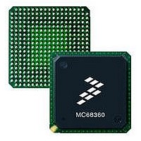
MC68360CAI25L Freescale Semiconductor, MC68360CAI25L Datasheet - Page 424

MC68360CAI25L
Manufacturer Part Number
MC68360CAI25L
Description
IC MPU QUICC 25MHZ 240-FQFP
Manufacturer
Freescale Semiconductor
Datasheets
1.MC68EN360VR25L.pdf
(14 pages)
2.MC68EN360VR25L.pdf
(2 pages)
3.MC68360AI25L.pdf
(962 pages)
4.MC68360CAI25L.pdf
(24 pages)
Specifications of MC68360CAI25L
Processor Type
M683xx 32-Bit
Speed
25MHz
Voltage
5V
Mounting Type
Surface Mount
Package / Case
240-FQFP
Family Name
M68000
Device Core
ColdFire
Device Core Size
32b
Frequency (max)
25MHz
Instruction Set Architecture
RISC
Supply Voltage 1 (typ)
5V
Operating Supply Voltage (max)
5.25V
Operating Supply Voltage (min)
4.75V
Operating Temp Range
-40C to 85C
Operating Temperature Classification
Industrial
Mounting
Surface Mount
Pin Count
240
Package Type
FQFP
Controller Family/series
68K
Core Size
32 Bit
Cpu Speed
25MHz
No. Of Timers
4
Embedded Interface Type
SCP, TDM
Digital Ic Case Style
FQFP
Supply Voltage Range
3V To 3.6V, 4.75V To 5.25V
Rohs Compliant
Yes
Lead Free Status / RoHS Status
Lead free / RoHS Compliant
Features
-
Lead Free Status / Rohs Status
Compliant
Available stocks
Company
Part Number
Manufacturer
Quantity
Price
Company:
Part Number:
MC68360CAI25L
Manufacturer:
SAMTEC
Quantity:
1 000
Company:
Part Number:
MC68360CAI25L
Manufacturer:
FREESCAL
Quantity:
717
Company:
Part Number:
MC68360CAI25L
Manufacturer:
Freescale Semiconductor
Quantity:
10 000
Part Number:
MC68360CAI25L
Manufacturer:
FREESCALE
Quantity:
20 000
- MC68EN360VR25L PDF datasheet
- MC68EN360VR25L PDF datasheet #2
- MC68360AI25L PDF datasheet #3
- MC68360CAI25L PDF datasheet #4
- Current page: 424 of 962
- Download datasheet (4Mb)
Serial Interface with Time Slot Assigner
7.8.8 Serial Interface Synchronization
On rev A and B of the QUICC, the SI would reset itself if an unexpected sync pulse was seen
during the middle of a time frame. This would cause the SI to sync again on the following
sync pulse but it would also lead to an unresolved loss of synchronization of an SCC or SMC
operating in transparent or GCI modes (assuming that SCC or SMC was receiving data from
the SI).
In revision C.1 and later of the QUICC, the SI will ignore this unexpected sync pulse and
synchronize on the next sync pulse (it will not reset itself). This may lead to a reception of
one or two “bad” slots but the SCC or SMC will remain synchronized.
7.8.9 NMSI Configuration
The SI supports an NMSI mode for each of the SCCs and SMCs. The decision of whether
to connect a given SCC to the NMSI is made in the SICR. The decision of whether to con-
nect a given SMC to the NMSI is made in the SIMODE register.
An SCC or SMC may be connected to the NMSI, regardless of which other channels are
connected to a TDM channel. The user should note, however, that NMSI pins may be mul-
tiplexed with other functions at the parallel I/O lines. Therefore, if a combination of TDM and
NMSI channels is used, the decision of which SCCs and SMCs to connect and where to con-
nect them should be made consulting the QUICC pinout. Generally speaking, the TDMa
channel is multiplexed with many of the SCC4 pins; whereas, the TDMb channel is multi-
plexed with many of the SCC3 pins.
The clocks that are provided to the SCCs and SMCs are derived from twelve sources: four
internal baud rate generators and eight external CLK pins (see Figure 7-35). There are two
main advantages to the bank-of-clocks approach. First, an SCC or SMC is not forced to
7-100
7. If the 1 GCI data clock is required, set PBPAR bit 11 and PBDIR bit 11, which
8. PCPAR bit 11 = 1. Configures L1RSYNCa.
9. SIGMR = $04. Enable TDMa (one static TDM).
10. 1SICMR is not used.
11. 1SISTR and SIRP do not need to be read, but can be used for debugging
12. 1Enable the SCC1 for HDLC operation (to handle the LAPD protocol of
configures L1CLKOa as an output.
information once the channels are enabled.
the D channel), set SCC2 and SCC4 as desired, and enable SMC1 for SCIT
operation.
Rev A mask is C63T
Rev B mask are C69T, and F35G
Current Rev C mask are E63C, E68C and F15W
Freescale Semiconductor, Inc.
For More Information On This Product,
MC68360 USER’S MANUAL
Go to: www.freescale.com
NOTE
Related parts for MC68360CAI25L
Image
Part Number
Description
Manufacturer
Datasheet
Request
R
Part Number:
Description:
Manufacturer:
Freescale Semiconductor, Inc
Datasheet:

Part Number:
Description:
MC68360 MC68360 Multiple Ethernet Channels on the QUICC
Manufacturer:
Motorola / Freescale Semiconductor

Part Number:
Description:
MC68360 Implementing an 8 bit Eprom for an MC68EC040-MC68360 System
Manufacturer:
Motorola / Freescale Semiconductor

Part Number:
Description:
MC68360 Interfacing the MC68060 to the MC68360
Manufacturer:
Motorola / Freescale Semiconductor

Part Number:
Description:
MC68360 MC68360 RAM Microcode Package Option Overview
Manufacturer:
Motorola / Freescale Semiconductor

Part Number:
Description:
MC68360 MC68360 CPM-CPU Interaction
Manufacturer:
Motorola / Freescale Semiconductor

Part Number:
Description:
MC68360 Interfacing SDRAM to the MC68360 QUICC Device
Manufacturer:
Motorola / Freescale Semiconductor

Part Number:
Description:
MC68360 Interfacing the QUICC to a MCM516400 (4Mx4 10-12 column-row) DRAM
Manufacturer:
Motorola / Freescale Semiconductor

Part Number:
Description:
MC68360 Interfacing the 68360 (QUICC) to T1-E1 Systems
Manufacturer:
Motorola / Freescale Semiconductor

Part Number:
Description:
MC68360 Multiple QUICC Design Concept
Manufacturer:
Motorola / Freescale Semiconductor
Part Number:
Description:
Manufacturer:
Freescale Semiconductor, Inc
Datasheet:
Part Number:
Description:
Manufacturer:
Freescale Semiconductor, Inc
Datasheet:
Part Number:
Description:
Manufacturer:
Freescale Semiconductor, Inc
Datasheet:
Part Number:
Description:
Manufacturer:
Freescale Semiconductor, Inc
Datasheet:
Part Number:
Description:
Manufacturer:
Freescale Semiconductor, Inc
Datasheet:


