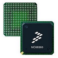
MC68360CAI25L Freescale Semiconductor, MC68360CAI25L Datasheet - Page 712

MC68360CAI25L
Manufacturer Part Number
MC68360CAI25L
Description
IC MPU QUICC 25MHZ 240-FQFP
Manufacturer
Freescale Semiconductor
Datasheets
1.MC68EN360VR25L.pdf
(14 pages)
2.MC68EN360VR25L.pdf
(2 pages)
3.MC68360AI25L.pdf
(962 pages)
4.MC68360CAI25L.pdf
(24 pages)
Specifications of MC68360CAI25L
Processor Type
M683xx 32-Bit
Speed
25MHz
Voltage
5V
Mounting Type
Surface Mount
Package / Case
240-FQFP
Family Name
M68000
Device Core
ColdFire
Device Core Size
32b
Frequency (max)
25MHz
Instruction Set Architecture
RISC
Supply Voltage 1 (typ)
5V
Operating Supply Voltage (max)
5.25V
Operating Supply Voltage (min)
4.75V
Operating Temp Range
-40C to 85C
Operating Temperature Classification
Industrial
Mounting
Surface Mount
Pin Count
240
Package Type
FQFP
Controller Family/series
68K
Core Size
32 Bit
Cpu Speed
25MHz
No. Of Timers
4
Embedded Interface Type
SCP, TDM
Digital Ic Case Style
FQFP
Supply Voltage Range
3V To 3.6V, 4.75V To 5.25V
Rohs Compliant
Yes
Lead Free Status / RoHS Status
Lead free / RoHS Compliant
Features
-
Lead Free Status / Rohs Status
Compliant
Available stocks
Company
Part Number
Manufacturer
Quantity
Price
Company:
Part Number:
MC68360CAI25L
Manufacturer:
SAMTEC
Quantity:
1 000
Company:
Part Number:
MC68360CAI25L
Manufacturer:
FREESCAL
Quantity:
717
Company:
Part Number:
MC68360CAI25L
Manufacturer:
Freescale Semiconductor
Quantity:
10 000
Part Number:
MC68360CAI25L
Manufacturer:
FREESCALE
Quantity:
20 000
- MC68EN360VR25L PDF datasheet
- MC68EN360VR25L PDF datasheet #2
- MC68360AI25L PDF datasheet #3
- MC68360CAI25L PDF datasheet #4
- Current page: 712 of 962
- Download datasheet (4Mb)
Scan Chain Test Access Port
The boundary scan bit definitions are listed in Table 8-2.
The first column in the table defines the bit’s ordinal position in the boundary scan register.
The shift register cell nearest TDO (i.e., first to be shifted out) is defined as bit 0; the last bit
to be shifted out is 195.
The second column references one of the four QUICC cell types depicted in Figure 8-3
through , which describe the cell structure for each type.
The third column lists the pin name for all pin-related cells or defines the name of bidirec-
tional control register bits.
The fourth column lists the pin type for convenience, where TS-Output indicates a three-
stateable output pin, I/O indicates a bidirectional pin, and OD-I/O denotes an open-drain
bidirectional pin.
The last column indicates the associated boundary scan register control bit for bidirectional,
three-state, and open-drain output pins.
Bidirectional pins include a single scan cell for data (IO.Cell) as depicted in Figure 8-6.
These bits are controlled by the cell shown in Figure 8-5. The value of the control bit deter-
mines whether the bidirectional pin is an input or an output. One or more bidirectional data
cells can be serially connected to a control cell as shown in Figure 8-7. Note that, when sam-
pling the bidirectional data cells, the cell data can be interpreted only after examining the IO
control cell to determine pin direction, and also note that the control cell captures the value
of the following cell.
8-4
g1.cntl
g2.cntl
g3.cntl
g4.cntl
g5.cntl
g6.cntl
g7.cntl
g8.cntl
g9.cntl
Name
Bit Number
Table 8-1. Boundary Scan Control Bits
Freescale Semiconductor, Inc.
13
16
18
23
27
29
2
5
8
For More Information On This Product,
MC68360 USER’S MANUAL
Go to: www.freescale.com
addh.cntl
g10.cntl
add.cntl
pahh.ctl
pbhh.ctl
g11.cnt
pahl.ctl
palh.ctl
Name
db.ctl
Bit Number
110
131
136
141
150
32
59
83
89
pchh.ctl
g12.cntl
g13.cntl
g14.cntl
pbhl.ctl
pblh.ctl
pchl.ctl
pclh.ctl
Name
Bit Number
155
159
170
174
179
188
191
194
Related parts for MC68360CAI25L
Image
Part Number
Description
Manufacturer
Datasheet
Request
R
Part Number:
Description:
Manufacturer:
Freescale Semiconductor, Inc
Datasheet:

Part Number:
Description:
MC68360 MC68360 Multiple Ethernet Channels on the QUICC
Manufacturer:
Motorola / Freescale Semiconductor

Part Number:
Description:
MC68360 Implementing an 8 bit Eprom for an MC68EC040-MC68360 System
Manufacturer:
Motorola / Freescale Semiconductor

Part Number:
Description:
MC68360 Interfacing the MC68060 to the MC68360
Manufacturer:
Motorola / Freescale Semiconductor

Part Number:
Description:
MC68360 MC68360 RAM Microcode Package Option Overview
Manufacturer:
Motorola / Freescale Semiconductor

Part Number:
Description:
MC68360 MC68360 CPM-CPU Interaction
Manufacturer:
Motorola / Freescale Semiconductor

Part Number:
Description:
MC68360 Interfacing SDRAM to the MC68360 QUICC Device
Manufacturer:
Motorola / Freescale Semiconductor

Part Number:
Description:
MC68360 Interfacing the QUICC to a MCM516400 (4Mx4 10-12 column-row) DRAM
Manufacturer:
Motorola / Freescale Semiconductor

Part Number:
Description:
MC68360 Interfacing the 68360 (QUICC) to T1-E1 Systems
Manufacturer:
Motorola / Freescale Semiconductor

Part Number:
Description:
MC68360 Multiple QUICC Design Concept
Manufacturer:
Motorola / Freescale Semiconductor
Part Number:
Description:
Manufacturer:
Freescale Semiconductor, Inc
Datasheet:
Part Number:
Description:
Manufacturer:
Freescale Semiconductor, Inc
Datasheet:
Part Number:
Description:
Manufacturer:
Freescale Semiconductor, Inc
Datasheet:
Part Number:
Description:
Manufacturer:
Freescale Semiconductor, Inc
Datasheet:
Part Number:
Description:
Manufacturer:
Freescale Semiconductor, Inc
Datasheet:


