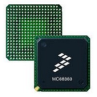
MC68360CAI25L Freescale Semiconductor, MC68360CAI25L Datasheet - Page 309

MC68360CAI25L
Manufacturer Part Number
MC68360CAI25L
Description
IC MPU QUICC 25MHZ 240-FQFP
Manufacturer
Freescale Semiconductor
Datasheets
1.MC68EN360VR25L.pdf
(14 pages)
2.MC68EN360VR25L.pdf
(2 pages)
3.MC68360AI25L.pdf
(962 pages)
4.MC68360CAI25L.pdf
(24 pages)
Specifications of MC68360CAI25L
Processor Type
M683xx 32-Bit
Speed
25MHz
Voltage
5V
Mounting Type
Surface Mount
Package / Case
240-FQFP
Family Name
M68000
Device Core
ColdFire
Device Core Size
32b
Frequency (max)
25MHz
Instruction Set Architecture
RISC
Supply Voltage 1 (typ)
5V
Operating Supply Voltage (max)
5.25V
Operating Supply Voltage (min)
4.75V
Operating Temp Range
-40C to 85C
Operating Temperature Classification
Industrial
Mounting
Surface Mount
Pin Count
240
Package Type
FQFP
Controller Family/series
68K
Core Size
32 Bit
Cpu Speed
25MHz
No. Of Timers
4
Embedded Interface Type
SCP, TDM
Digital Ic Case Style
FQFP
Supply Voltage Range
3V To 3.6V, 4.75V To 5.25V
Rohs Compliant
Yes
Lead Free Status / RoHS Status
Lead free / RoHS Compliant
Features
-
Lead Free Status / Rohs Status
Compliant
Available stocks
Company
Part Number
Manufacturer
Quantity
Price
Company:
Part Number:
MC68360CAI25L
Manufacturer:
SAMTEC
Quantity:
1 000
Company:
Part Number:
MC68360CAI25L
Manufacturer:
FREESCAL
Quantity:
717
Company:
Part Number:
MC68360CAI25L
Manufacturer:
Freescale Semiconductor
Quantity:
10 000
Part Number:
MC68360CAI25L
Manufacturer:
FREESCALE
Quantity:
20 000
- MC68EN360VR25L PDF datasheet
- MC68EN360VR25L PDF datasheet #2
- MC68360AI25L PDF datasheet #3
- MC68360CAI25L PDF datasheet #4
- Current page: 309 of 962
- Download datasheet (4Mb)
The following bits are used for DRAM bank properties:
PGS2–PGS0—Page Size
DPS1–DPS0—DRAM Port Size
This attribute determines the page size for the DRAM controller (see Table 6-9). The page
size is the smallest DRAM size the user needs to support with page mode capability.
For instance, PGS = 001 (256K) should be used for a 32-bit-wide memory composed of
four 256K
teen 256K
This attribute determines the DRAM bank port size (see Table 6-10). The DRAM controller
asserts the appropriate DSACKx lines according to these bits. If an MC68EC040 access
is performed using this DRAM bank and SPS = 00 or 01, the DRAM controller operates
the same way, but asserts TA instead of DSACK.
The internal DRAM address multiplexer and the page logic sup-
port only a port size of 32 bits or 16 bits. An 8-bit DRAM port size
is not allowed.
The DRAM controller does not support an external DSACKx re-
sponse for a bank on which page mode is used. Also, an exter-
nal DSACK response may not occur before RAS is asserted.
PGS2-PGS0
8 devices, a 16-bit-wide memory composed of two 256K
1 devices. In all cases, the width of the DRAMs is irrelevant.
000
001
010
011
100
101
110
110
Freescale Semiconductor, Inc.
For More Information On This Product,
A11-25(32), A10-25(16)
A11-25(32), A10-25(16)
A12-25(32), A11-25(16)
A12-25(32), A11-25(16)
A13-25(32), A12-25(16)
A13-25(32), A12-25(16)
A14-25(32), A13-25(16)
A10-25(32), A9-25(16)
Address Lines Used
DPS1–DPS0
Table 6-10. DRAM Port Size
Table 6-9. DRAM Page Size
MC68360 USER’S MANUAL
00
01
10
11
Go to: www.freescale.com
NOTES
DRAM Port Size Is 32 Bits
DRAM Port Size Is 16 Bits
External DSACKx Support
Reserved
# Address/Page in Page Compare
Result
1024 Addresses
1024 Addresses
2048 Addresses
2048 Addresses
4096 Addresses
256 Addresses
512 Addresses
512 Addresses
System Integration Module (SIM60)
8 devices, or six-
Related parts for MC68360CAI25L
Image
Part Number
Description
Manufacturer
Datasheet
Request
R
Part Number:
Description:
Manufacturer:
Freescale Semiconductor, Inc
Datasheet:

Part Number:
Description:
MC68360 MC68360 Multiple Ethernet Channels on the QUICC
Manufacturer:
Motorola / Freescale Semiconductor

Part Number:
Description:
MC68360 Implementing an 8 bit Eprom for an MC68EC040-MC68360 System
Manufacturer:
Motorola / Freescale Semiconductor

Part Number:
Description:
MC68360 Interfacing the MC68060 to the MC68360
Manufacturer:
Motorola / Freescale Semiconductor

Part Number:
Description:
MC68360 MC68360 RAM Microcode Package Option Overview
Manufacturer:
Motorola / Freescale Semiconductor

Part Number:
Description:
MC68360 MC68360 CPM-CPU Interaction
Manufacturer:
Motorola / Freescale Semiconductor

Part Number:
Description:
MC68360 Interfacing SDRAM to the MC68360 QUICC Device
Manufacturer:
Motorola / Freescale Semiconductor

Part Number:
Description:
MC68360 Interfacing the QUICC to a MCM516400 (4Mx4 10-12 column-row) DRAM
Manufacturer:
Motorola / Freescale Semiconductor

Part Number:
Description:
MC68360 Interfacing the 68360 (QUICC) to T1-E1 Systems
Manufacturer:
Motorola / Freescale Semiconductor

Part Number:
Description:
MC68360 Multiple QUICC Design Concept
Manufacturer:
Motorola / Freescale Semiconductor
Part Number:
Description:
Manufacturer:
Freescale Semiconductor, Inc
Datasheet:
Part Number:
Description:
Manufacturer:
Freescale Semiconductor, Inc
Datasheet:
Part Number:
Description:
Manufacturer:
Freescale Semiconductor, Inc
Datasheet:
Part Number:
Description:
Manufacturer:
Freescale Semiconductor, Inc
Datasheet:
Part Number:
Description:
Manufacturer:
Freescale Semiconductor, Inc
Datasheet:


