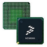
MC68360CAI25L Freescale Semiconductor, MC68360CAI25L Datasheet - Page 82

MC68360CAI25L
Manufacturer Part Number
MC68360CAI25L
Description
IC MPU QUICC 25MHZ 240-FQFP
Manufacturer
Freescale Semiconductor
Datasheets
1.MC68EN360VR25L.pdf
(14 pages)
2.MC68EN360VR25L.pdf
(2 pages)
3.MC68360AI25L.pdf
(962 pages)
4.MC68360CAI25L.pdf
(24 pages)
Specifications of MC68360CAI25L
Processor Type
M683xx 32-Bit
Speed
25MHz
Voltage
5V
Mounting Type
Surface Mount
Package / Case
240-FQFP
Family Name
M68000
Device Core
ColdFire
Device Core Size
32b
Frequency (max)
25MHz
Instruction Set Architecture
RISC
Supply Voltage 1 (typ)
5V
Operating Supply Voltage (max)
5.25V
Operating Supply Voltage (min)
4.75V
Operating Temp Range
-40C to 85C
Operating Temperature Classification
Industrial
Mounting
Surface Mount
Pin Count
240
Package Type
FQFP
Controller Family/series
68K
Core Size
32 Bit
Cpu Speed
25MHz
No. Of Timers
4
Embedded Interface Type
SCP, TDM
Digital Ic Case Style
FQFP
Supply Voltage Range
3V To 3.6V, 4.75V To 5.25V
Rohs Compliant
Yes
Lead Free Status / RoHS Status
Lead free / RoHS Compliant
Features
-
Lead Free Status / Rohs Status
Compliant
Available stocks
Company
Part Number
Manufacturer
Quantity
Price
Company:
Part Number:
MC68360CAI25L
Manufacturer:
SAMTEC
Quantity:
1 000
Company:
Part Number:
MC68360CAI25L
Manufacturer:
FREESCAL
Quantity:
717
Company:
Part Number:
MC68360CAI25L
Manufacturer:
Freescale Semiconductor
Quantity:
10 000
Part Number:
MC68360CAI25L
Manufacturer:
FREESCALE
Quantity:
20 000
- MC68EN360VR25L PDF datasheet
- MC68EN360VR25L PDF datasheet #2
- MC68360AI25L PDF datasheet #3
- MC68360CAI25L PDF datasheet #4
- Current page: 82 of 962
- Download datasheet (4Mb)
Bus Operation
appropriate timing described in this section and in Section 10 Electrical Characteristics.
Additionally, BERR and HALT can be asserted together to indicate a retry termination. Refer
to 4.5 Bus Exception Control Cycles for additional information on the use of these signals.
See the memory controller description in Section 6 System Integration Module (SIM60) for
precautions about asserting BERR externally too early during DRAM and SRAM cycles con-
trolled by the memory controller.
The internal bus monitor can be used to generate the BERR signal for internal and external
transfers in all the following descriptions.
4.1.9.3 AUTOVECTOR (AVEC). This signal can be used to terminate interrupt acknowl-
edge cycles, indicating that the QUICC should internally generate a vector (autovector)
number to locate an interrupt handler routine. AVEC can be generated either externally or
internally by the SIM60 (refer to Section 6 System Integration Module (SIM60) for additional
information). AVEC is ignored during all other bus cycles.
4.2 DATA TRANSFER MECHANISM
The QUICC supports byte, word, and long-word operands, allowing access to 8-,16-, and
32-bit data ports through the use of asynchronous cycles controlled by DSACK1 and
DSACK0. The QUICC also supports byte, word, and long-word operands, allowing access
to 8-, 16, and 32-bit data ports through the use of synchronous cycles controlled by the fast-
termination capability of the SIM60.
4.2.1 Dynamic Bus Sizing
The QUICC dynamically interprets the port size of the addressed device during each bus
cycle, allowing operand transfers to or from 8-, 16-, and 32-bit ports. During an operand
transfer cycle, the slave device signals its port size (byte, word, or long word) and indicates
completion of the bus cycle to the QUICC through the use of the DSACKx inputs. Refer to
Table 4-2 for DSACKx encoding.
For example, if the QUICC is executing an instruction that reads a long-word operand from
a long-word aligned address, it attempts to read 32 bits during the first bus cycle. (Refer to
4.2.2 Misaligned Operands for the case of a word or byte address.) If the port responds that
it is 32 bits wide, the QUICC latches all 32 bits of data and continues with the next operation.
If the port responds that it is 16 bits wide, the QUICC latches the 16 bits of valid data and
runs another bus cycle to obtain the other 16 bits. The operation for an 8-bit port is similar,
but requires four read cycles. The addressed device uses the DSACKx signals to indicate
4-6
DSACK1
1
1
0
0
Freescale Semiconductor, Inc.
For More Information On This Product,
DSACK0
Table 4-2. DSACKx Encoding
1
0
1
0
MC68360 USER’S MANUAL
Go to: www.freescale.com
Insert Wait States in Current Bus Cycle
Complete Cycle—Data Bus Port Size is 8 Bits
Complete Cycle—Data Bus Port Size is 16 Bits
Complete Cycle—Data Bus Port Size is 32 Bits
Result
Related parts for MC68360CAI25L
Image
Part Number
Description
Manufacturer
Datasheet
Request
R
Part Number:
Description:
Manufacturer:
Freescale Semiconductor, Inc
Datasheet:

Part Number:
Description:
MC68360 MC68360 Multiple Ethernet Channels on the QUICC
Manufacturer:
Motorola / Freescale Semiconductor

Part Number:
Description:
MC68360 Implementing an 8 bit Eprom for an MC68EC040-MC68360 System
Manufacturer:
Motorola / Freescale Semiconductor

Part Number:
Description:
MC68360 Interfacing the MC68060 to the MC68360
Manufacturer:
Motorola / Freescale Semiconductor

Part Number:
Description:
MC68360 MC68360 RAM Microcode Package Option Overview
Manufacturer:
Motorola / Freescale Semiconductor

Part Number:
Description:
MC68360 MC68360 CPM-CPU Interaction
Manufacturer:
Motorola / Freescale Semiconductor

Part Number:
Description:
MC68360 Interfacing SDRAM to the MC68360 QUICC Device
Manufacturer:
Motorola / Freescale Semiconductor

Part Number:
Description:
MC68360 Interfacing the QUICC to a MCM516400 (4Mx4 10-12 column-row) DRAM
Manufacturer:
Motorola / Freescale Semiconductor

Part Number:
Description:
MC68360 Interfacing the 68360 (QUICC) to T1-E1 Systems
Manufacturer:
Motorola / Freescale Semiconductor

Part Number:
Description:
MC68360 Multiple QUICC Design Concept
Manufacturer:
Motorola / Freescale Semiconductor
Part Number:
Description:
Manufacturer:
Freescale Semiconductor, Inc
Datasheet:
Part Number:
Description:
Manufacturer:
Freescale Semiconductor, Inc
Datasheet:
Part Number:
Description:
Manufacturer:
Freescale Semiconductor, Inc
Datasheet:
Part Number:
Description:
Manufacturer:
Freescale Semiconductor, Inc
Datasheet:
Part Number:
Description:
Manufacturer:
Freescale Semiconductor, Inc
Datasheet:


