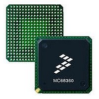
MC68360CAI25L Freescale Semiconductor, MC68360CAI25L Datasheet - Page 332

MC68360CAI25L
Manufacturer Part Number
MC68360CAI25L
Description
IC MPU QUICC 25MHZ 240-FQFP
Manufacturer
Freescale Semiconductor
Datasheets
1.MC68EN360VR25L.pdf
(14 pages)
2.MC68EN360VR25L.pdf
(2 pages)
3.MC68360AI25L.pdf
(962 pages)
4.MC68360CAI25L.pdf
(24 pages)
Specifications of MC68360CAI25L
Processor Type
M683xx 32-Bit
Speed
25MHz
Voltage
5V
Mounting Type
Surface Mount
Package / Case
240-FQFP
Family Name
M68000
Device Core
ColdFire
Device Core Size
32b
Frequency (max)
25MHz
Instruction Set Architecture
RISC
Supply Voltage 1 (typ)
5V
Operating Supply Voltage (max)
5.25V
Operating Supply Voltage (min)
4.75V
Operating Temp Range
-40C to 85C
Operating Temperature Classification
Industrial
Mounting
Surface Mount
Pin Count
240
Package Type
FQFP
Controller Family/series
68K
Core Size
32 Bit
Cpu Speed
25MHz
No. Of Timers
4
Embedded Interface Type
SCP, TDM
Digital Ic Case Style
FQFP
Supply Voltage Range
3V To 3.6V, 4.75V To 5.25V
Rohs Compliant
Yes
Lead Free Status / RoHS Status
Lead free / RoHS Compliant
Features
-
Lead Free Status / Rohs Status
Compliant
Available stocks
Company
Part Number
Manufacturer
Quantity
Price
Company:
Part Number:
MC68360CAI25L
Manufacturer:
SAMTEC
Quantity:
1 000
Company:
Part Number:
MC68360CAI25L
Manufacturer:
FREESCAL
Quantity:
717
Company:
Part Number:
MC68360CAI25L
Manufacturer:
Freescale Semiconductor
Quantity:
10 000
Part Number:
MC68360CAI25L
Manufacturer:
FREESCALE
Quantity:
20 000
- MC68EN360VR25L PDF datasheet
- MC68EN360VR25L PDF datasheet #2
- MC68360AI25L PDF datasheet #3
- MC68360CAI25L PDF datasheet #4
- Current page: 332 of 962
- Download datasheet (4Mb)
Dual-Port RAM
7.2.1 Command Register Examples
To perform a complete reset of the CP, the value $8001 should be written to the CR. Fol-
lowing this command, the CR will return the value $0000 in two clocks.
To execute an ENTER HUNT MODE command to SCC3, the value $0381 should be written
to the CR. While the command is executing, the CR will return the value $0381. When the
command has been completely executed, the CR will return the value $0380.
7.2.2 Command Execution Latency
The worst-case command execution latency is 120 clocks. The typical command execution
latency is about 40 clocks.
7.3 DUAL-PORT RAM
The CPM has 2560 bytes of static RAM configured as dual-port memory. The dual-port RAM
memory map is shown in Figure 7-2, and a block diagram is shown in Figure 7-3.
7-8
0 = The CP is ready to receive a new command.
1 = The CR contains a command that the CP is currently processing. The CP clears
this bit at the end of the command execution or after reset.
MBAR POINTS
TO THE BASE
Figure 7-2. Dual-Port RAM Memory Map
Freescale Semiconductor, Inc.
For More Information On This Product,
0.5K
1.5K
2.5K
3.5K
4K
1K
2K
3K
MC68360 USER’S MANUAL
0
Go to: www.freescale.com
BDs/DATA IN ANY UNUSED SPACE
PARAMETER RAM—768 BYTES
BDs/DATA/UCODE—512 BYTES
BDs/DATA/UCODE—256 BYTES
BDs/DATA/UCODE—512 BYTES
BDs/DATA—512 BYTES
TOTAL 2560 BYTES
Related parts for MC68360CAI25L
Image
Part Number
Description
Manufacturer
Datasheet
Request
R
Part Number:
Description:
Manufacturer:
Freescale Semiconductor, Inc
Datasheet:

Part Number:
Description:
MC68360 MC68360 Multiple Ethernet Channels on the QUICC
Manufacturer:
Motorola / Freescale Semiconductor

Part Number:
Description:
MC68360 Implementing an 8 bit Eprom for an MC68EC040-MC68360 System
Manufacturer:
Motorola / Freescale Semiconductor

Part Number:
Description:
MC68360 Interfacing the MC68060 to the MC68360
Manufacturer:
Motorola / Freescale Semiconductor

Part Number:
Description:
MC68360 MC68360 RAM Microcode Package Option Overview
Manufacturer:
Motorola / Freescale Semiconductor

Part Number:
Description:
MC68360 MC68360 CPM-CPU Interaction
Manufacturer:
Motorola / Freescale Semiconductor

Part Number:
Description:
MC68360 Interfacing SDRAM to the MC68360 QUICC Device
Manufacturer:
Motorola / Freescale Semiconductor

Part Number:
Description:
MC68360 Interfacing the QUICC to a MCM516400 (4Mx4 10-12 column-row) DRAM
Manufacturer:
Motorola / Freescale Semiconductor

Part Number:
Description:
MC68360 Interfacing the 68360 (QUICC) to T1-E1 Systems
Manufacturer:
Motorola / Freescale Semiconductor

Part Number:
Description:
MC68360 Multiple QUICC Design Concept
Manufacturer:
Motorola / Freescale Semiconductor
Part Number:
Description:
Manufacturer:
Freescale Semiconductor, Inc
Datasheet:
Part Number:
Description:
Manufacturer:
Freescale Semiconductor, Inc
Datasheet:
Part Number:
Description:
Manufacturer:
Freescale Semiconductor, Inc
Datasheet:
Part Number:
Description:
Manufacturer:
Freescale Semiconductor, Inc
Datasheet:
Part Number:
Description:
Manufacturer:
Freescale Semiconductor, Inc
Datasheet:


