DEMO9S08LC60 Freescale Semiconductor, DEMO9S08LC60 Datasheet - Page 139
DEMO9S08LC60
Manufacturer Part Number
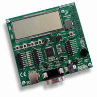
DEMO9S08LC60
Description
BOARD DEMO FOR 9S08LC60
Manufacturer
Freescale Semiconductor
Type
MCUr
Datasheets
1.DEMO9S08LC60.pdf
(360 pages)
2.DEMO9S08LC60.pdf
(32 pages)
3.DEMO9S08LC60.pdf
(2 pages)
Specifications of DEMO9S08LC60
Contents
Evaluation Board
Processor To Be Evaluated
MC9S08LC60
Interface Type
RS-232, USB
Silicon Manufacturer
Freescale
Core Architecture
HCS08
Core Sub-architecture
HCS08
Silicon Core Number
MC9S08
Silicon Family Name
S08LC
Rohs Compliant
Yes
For Use With/related Products
MC9S08LC60
Lead Free Status / RoHS Status
Lead free / RoHS Compliant


9.4.1.2
Because a single frontplane driver is configured to drive more and more individual LCD segments, more
voltage levels are required to generate the appropriate waveforms to drive the segment. The LCD module
is designed to operate using the 1/3 bias mode.
Defined by
9.4.1.3
The LCD module is designed to operate using a 32.768-kHz clock input. Two possible clock sources are
available to the LCD module has which are selectable by configuration of the SOURCE bit in the
LCDCLKS register. The two clock sources include:
Figure 9-10
LCD frame frequency and blink frequency clock source. The LCD blink frequency is discussed in
Section 9.4.3.2, “Blink
Because the clock sources may not be approximately 32.768 kHz, the DIV16 bit and CLKADJ[5:0] bit
field are provided as a clock divider mechanism that can be used to make LCD module clock source
adjustments in order to achieve the required 32.768-kHz LCD module clock input, LCDCLK.
provides calculations of LCDCLK using different values of DIV16 and CLKADJ[5:0] for a range of clock
inputs frequencies. Using an external 32.768-kHz clock input is required for reduced power consumption
applications.
Freescale Semiconductor
External Clock = 32.768 kHz
•
•
Internal Clock
External crystal (SOURCE = 0)
Internal ICG (SOURCE = 1)
Equation
shows the LCD clock tree. The clock tree shows the two possible clock sources and shows the
LCD Bias
LCD Module
SOURCE
9-5, the bias indicates the number of voltage levels used to power the LCD display.
Frequency.”
MC9S08LC60 Series Data Sheet: Technical Data, Rev. 4
Waveform Base Clock and
÷16
DIV16
1 / (voltage level – 1)
Figure 9-10. LCD Clock Tree
÷(1+CLKADJ[5:0])
CLKADJ[5:0]
LCDCLK
LCD Charge Pump Clock
Source
÷2
(1+CPCADJ[1:0])
÷8
Frame Frequency
÷6
Chapter 9 Liquid Crystal Display Driver (S08LCDV1)
LCLK[2:0]
÷(2
CPCADJ[1:0]
LCLK[2:0]
)
÷2
LCD Base Frequency
Source
÷(2
5+BRATE[2:0]
BRATE[2:0]
)
Table 9-14
Blink Rate
Source
÷2
Eqn. 9-5
139
Related parts for DEMO9S08LC60
Image
Part Number
Description
Manufacturer
Datasheet
Request
R

Part Number:
Description:
Manufacturer:
Freescale Semiconductor, Inc
Datasheet:
Part Number:
Description:
Manufacturer:
Freescale Semiconductor, Inc
Datasheet:
Part Number:
Description:
Manufacturer:
Freescale Semiconductor, Inc
Datasheet:
Part Number:
Description:
Manufacturer:
Freescale Semiconductor, Inc
Datasheet:
Part Number:
Description:
Manufacturer:
Freescale Semiconductor, Inc
Datasheet:
Part Number:
Description:
Manufacturer:
Freescale Semiconductor, Inc
Datasheet:
Part Number:
Description:
Manufacturer:
Freescale Semiconductor, Inc
Datasheet:
Part Number:
Description:
Manufacturer:
Freescale Semiconductor, Inc
Datasheet:
Part Number:
Description:
Manufacturer:
Freescale Semiconductor, Inc
Datasheet:
Part Number:
Description:
Manufacturer:
Freescale Semiconductor, Inc
Datasheet:
Part Number:
Description:
Manufacturer:
Freescale Semiconductor, Inc
Datasheet:
Part Number:
Description:
Manufacturer:
Freescale Semiconductor, Inc
Datasheet:
Part Number:
Description:
Manufacturer:
Freescale Semiconductor, Inc
Datasheet:
Part Number:
Description:
Manufacturer:
Freescale Semiconductor, Inc
Datasheet:
Part Number:
Description:
Manufacturer:
Freescale Semiconductor, Inc
Datasheet: