DEMO9S08LC60 Freescale Semiconductor, DEMO9S08LC60 Datasheet - Page 224
DEMO9S08LC60
Manufacturer Part Number
DEMO9S08LC60
Description
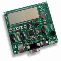
BOARD DEMO FOR 9S08LC60
Manufacturer
Freescale Semiconductor
Type
MCUr
Datasheets
1.DEMO9S08LC60.pdf
(360 pages)
2.DEMO9S08LC60.pdf
(32 pages)
3.DEMO9S08LC60.pdf
(2 pages)
Specifications of DEMO9S08LC60
Contents
Evaluation Board
Processor To Be Evaluated
MC9S08LC60
Interface Type
RS-232, USB
Silicon Manufacturer
Freescale
Core Architecture
HCS08
Core Sub-architecture
HCS08
Silicon Core Number
MC9S08
Silicon Family Name
S08LC
Rohs Compliant
Yes
For Use With/related Products
MC9S08LC60
Lead Free Status / RoHS Status
Lead free / RoHS Compliant


Chapter 12 Serial Communications Interface (S08SCIV3)
12.2.5
This register has one read-only status flag. Writes have no effect.
12.2.6
224
Reset
Reset
BRK13
Field
Field
RAF
R8
T8
2
0
7
6
W
W
R
R
SCI Status Register 2 (SCIS2)
SCI Control Register 3 (SCIC3)
Break Character Length — BRK13 is used to select a longer break character length. Detection of a framing
error is not affected by the state of this bit.
0 Break character is 10 bit times (11 if M = 1)
1 Break character is 13 bit times (14 if M = 1)
Receiver Active Flag — RAF is set when the SCI receiver detects the beginning of a valid start bit, and RAF is
cleared automatically when the receiver detects an idle line. This status flag can be used to check whether an
SCI character is being received before instructing the MCU to go to stop mode.
0 SCI receiver idle waiting for a start bit.
1 SCI receiver active (RxD input not idle).
Ninth Data Bit for Receiver — When the SCI is configured for 9-bit data (M = 1), R8 can be thought of as a
ninth receive data bit to the left of the MSB of the buffered data in the SCID register. When reading 9-bit data,
read R8 before reading SCID because reading SCID completes automatic flag clearing sequences which could
allow R8 and SCID to be overwritten with new data.
Ninth Data Bit for Transmitter — When the SCI is configured for 9-bit data (M = 1), T8 may be thought of as a
ninth transmit data bit to the left of the MSB of the data in the SCID register. When writing 9-bit data, the entire
9-bit value is transferred to the SCI shift register after SCID is written so T8 should be written (if it needs to
change from its previous value) before SCID is written. If T8 does not need to change in the new value (such as
when it is used to generate mark or space parity), it need not be written each time SCID is written.
R8
0
0
0
7
7
= Unimplemented or Reserved
= Unimplemented or Reserved
T8
0
0
0
6
6
MC9S08LC60 Series Data Sheet: Technical Data, Rev. 4
Table 12-7. SCIC3 Register Field Descriptions
Table 12-6. SCIS2 Register Field Descriptions
Figure 12-11. SCI Control Register 3 (SCIC3)
Figure 12-10. SCI Status Register 2 (SCIS2)
TXDIR
0
0
0
5
5
TXINV
0
0
0
4
4
Description
Description
ORIE
3
0
0
3
0
BRK13
NEIE
0
0
2
2
Freescale Semiconductor
FEIE
0
0
0
1
1
PEIE
RAF
0
0
0
0
Related parts for DEMO9S08LC60
Image
Part Number
Description
Manufacturer
Datasheet
Request
R

Part Number:
Description:
Manufacturer:
Freescale Semiconductor, Inc
Datasheet:
Part Number:
Description:
Manufacturer:
Freescale Semiconductor, Inc
Datasheet:
Part Number:
Description:
Manufacturer:
Freescale Semiconductor, Inc
Datasheet:
Part Number:
Description:
Manufacturer:
Freescale Semiconductor, Inc
Datasheet:
Part Number:
Description:
Manufacturer:
Freescale Semiconductor, Inc
Datasheet:
Part Number:
Description:
Manufacturer:
Freescale Semiconductor, Inc
Datasheet:
Part Number:
Description:
Manufacturer:
Freescale Semiconductor, Inc
Datasheet:
Part Number:
Description:
Manufacturer:
Freescale Semiconductor, Inc
Datasheet:
Part Number:
Description:
Manufacturer:
Freescale Semiconductor, Inc
Datasheet:
Part Number:
Description:
Manufacturer:
Freescale Semiconductor, Inc
Datasheet:
Part Number:
Description:
Manufacturer:
Freescale Semiconductor, Inc
Datasheet:
Part Number:
Description:
Manufacturer:
Freescale Semiconductor, Inc
Datasheet:
Part Number:
Description:
Manufacturer:
Freescale Semiconductor, Inc
Datasheet:
Part Number:
Description:
Manufacturer:
Freescale Semiconductor, Inc
Datasheet:
Part Number:
Description:
Manufacturer:
Freescale Semiconductor, Inc
Datasheet: