DEMO9S08LC60 Freescale Semiconductor, DEMO9S08LC60 Datasheet - Page 149
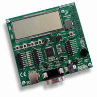
DEMO9S08LC60
Manufacturer Part Number
DEMO9S08LC60
Description
BOARD DEMO FOR 9S08LC60
Manufacturer
Freescale Semiconductor
Type
MCUr
Datasheets
1.DEMO9S08LC60.pdf
(360 pages)
2.DEMO9S08LC60.pdf
(32 pages)
3.DEMO9S08LC60.pdf
(2 pages)
Specifications of DEMO9S08LC60
Contents
Evaluation Board
Processor To Be Evaluated
MC9S08LC60
Interface Type
RS-232, USB
Silicon Manufacturer
Freescale
Core Architecture
HCS08
Core Sub-architecture
HCS08
Silicon Core Number
MC9S08
Silicon Family Name
S08LC
Rohs Compliant
Yes
For Use With/related Products
MC9S08LC60
Lead Free Status / RoHS Status
Lead free / RoHS Compliant


9.4.2
For a segment on the LCD panel to be displayed, data must be written to the LCDRAM registers. Each bit
in the LCDRAM registers correspond to a segment on the LCD panel.
The LCDRAM registers provide access to two different register groups depending on the state of the
LCDDRMS bit in the LCDCMD register. If LCDDRMS = 0, the LCDRAM register accesses a register
bank that controls the on/off state for frontplane drivers
accesses a register bank that enables the blink mode for each individual LCD segment
If LCDDRMS = 0, when the LCDEN bit is set and the corresponding FP[31:0]EN bit is set, writing a 1 to
a given LCDRAM location will result in the corresponding display segment being driven with a
differential root mean square (RMS) voltage necessary to turn the segment on.Writing a 0 to a given
location will result in the corresponding display segment being driven with a differential RMS voltage
necessary to turn the segment off.
The LCDRAM is a dual port RAM that interfaces with the internal address and data buses of the MCU.
When LCDEN = 0, the LCDRAM registers can be used as on-chip RAM. Writing or reading of the
LCDEN bit does not change the contents of the LCDRAM registers.After a reset, the LCDRAM contents
will be indeterminate.
9.4.2.1
The LCD module data register clear command deasserts all accessible bits in the LCDRAM registers.
LCDDRMS bit in the LCDCMD register determines which LCDRAM registers bits are accessible.To
clear all LCD segment blink enables in the LCDRAM registers, the LCDCLR bit must be asserted only
when the LCDDRMS bit is asserted. To clear the entire LCD display, the LCDCLR bit must be asserted
only when the LCDDRMS bit is deasserted.
9.4.2.2
The LCD module display blank command clears all segments in the LCD display regardless of the contents
of the LCDRAM registers or the state of the LCDDRMS bit. This bit does not disable the LCD module
timing generator. Writing or reading of the BLANK bit does not change the contents of the LCDRAM
registers.
9.4.3
The LCD module LCD panel blink capabilities are very flexible. The LCD module can be configured to
blink either individual LCD segments or the entire LCD panel. The blink rate frequency is configured
using the BRATE[2:0] bit field.
The LCD will blink at the configured frequency while the BLINK bit in the LCDBCTL register is set to 1.
When the BLINK bit is modified to start or stop the LCD display blinking, the BLINK command change
takes place at the beginning of the next LCD frame cycle.
Freescale Semiconductor
LCDRAM Registers
LCD Blinking
LCDRAM Data Clear Command
LCDRAM Data Blank Command
MC9S08LC60 Series Data Sheet: Technical Data, Rev. 4
.
If LCDDRMS = 1, the LCDRAM register bank
Chapter 9 Liquid Crystal Display Driver (S08LCDV1)
.
149
Related parts for DEMO9S08LC60
Image
Part Number
Description
Manufacturer
Datasheet
Request
R

Part Number:
Description:
Manufacturer:
Freescale Semiconductor, Inc
Datasheet:
Part Number:
Description:
Manufacturer:
Freescale Semiconductor, Inc
Datasheet:
Part Number:
Description:
Manufacturer:
Freescale Semiconductor, Inc
Datasheet:
Part Number:
Description:
Manufacturer:
Freescale Semiconductor, Inc
Datasheet:
Part Number:
Description:
Manufacturer:
Freescale Semiconductor, Inc
Datasheet:
Part Number:
Description:
Manufacturer:
Freescale Semiconductor, Inc
Datasheet:
Part Number:
Description:
Manufacturer:
Freescale Semiconductor, Inc
Datasheet:
Part Number:
Description:
Manufacturer:
Freescale Semiconductor, Inc
Datasheet:
Part Number:
Description:
Manufacturer:
Freescale Semiconductor, Inc
Datasheet:
Part Number:
Description:
Manufacturer:
Freescale Semiconductor, Inc
Datasheet:
Part Number:
Description:
Manufacturer:
Freescale Semiconductor, Inc
Datasheet:
Part Number:
Description:
Manufacturer:
Freescale Semiconductor, Inc
Datasheet:
Part Number:
Description:
Manufacturer:
Freescale Semiconductor, Inc
Datasheet:
Part Number:
Description:
Manufacturer:
Freescale Semiconductor, Inc
Datasheet:
Part Number:
Description:
Manufacturer:
Freescale Semiconductor, Inc
Datasheet: