DEMO9S08LC60 Freescale Semiconductor, DEMO9S08LC60 Datasheet - Page 221
DEMO9S08LC60
Manufacturer Part Number
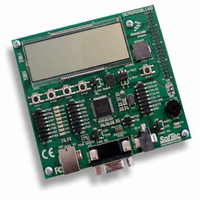
DEMO9S08LC60
Description
BOARD DEMO FOR 9S08LC60
Manufacturer
Freescale Semiconductor
Type
MCUr
Datasheets
1.DEMO9S08LC60.pdf
(360 pages)
2.DEMO9S08LC60.pdf
(32 pages)
3.DEMO9S08LC60.pdf
(2 pages)
Specifications of DEMO9S08LC60
Contents
Evaluation Board
Processor To Be Evaluated
MC9S08LC60
Interface Type
RS-232, USB
Silicon Manufacturer
Freescale
Core Architecture
HCS08
Core Sub-architecture
HCS08
Silicon Core Number
MC9S08
Silicon Family Name
S08LC
Rohs Compliant
Yes
For Use With/related Products
MC9S08LC60
Lead Free Status / RoHS Status
Lead free / RoHS Compliant


12.2.3
This register can be read or written at any time.
Freescale Semiconductor
Reset
Field
Field
TCIE
ILIE
TIE
RIE
PE
PT
TE
1
0
7
6
5
4
3
W
R
SCI Control Register 2 (SCIC2)
Parity Enable — Enables hardware parity generation and checking. When parity is enabled, the most significant
bit (MSB) of the data character (eighth or ninth data bit) is treated as the parity bit.
0 No hardware parity generation or checking.
1 Parity enabled.
Parity Type — Provided parity is enabled (PE = 1), this bit selects even or odd parity. Odd parity means the total
number of 1s in the data character, including the parity bit, is odd. Even parity means the total number of 1s in
the data character, including the parity bit, is even.
0 Even parity.
1 Odd parity.
TIE
Transmit Interrupt Enable (for TDRE)
0 Hardware interrupts from TDRE disabled (use polling).
1 Hardware interrupt requested when TDRE flag is 1.
Transmission Complete Interrupt Enable (for TC)
0 Hardware interrupts from TC disabled (use polling).
1 Hardware interrupt requested when TC flag is 1.
Receiver Interrupt Enable (for RDRF)
0 Hardware interrupts from RDRF disabled (use polling).
1 Hardware interrupt requested when RDRF flag is 1.
Idle Line Interrupt Enable (for IDLE)
0 Hardware interrupts from IDLE disabled (use polling).
1 Hardware interrupt requested when IDLE flag is 1.
Transmitter Enable
0 Transmitter off.
1 Transmitter on.
TE must be 1 in order to use the SCI transmitter. When TE = 1, the SCI forces the TxD pin to act as an output
for the SCI system.
When the SCI is configured for single-wire operation (LOOPS = RSRC = 1), TXDIR controls the direction of
traffic on the single SCI communication line (TxD pin).
TE also can be used to queue an idle character by writing TE = 0 then TE = 1 while a transmission is in progress.
Refer to
When TE is written to 0, the transmitter keeps control of the port TxD pin until any data, queued idle, or queued
break character finishes transmitting before allowing the pin to revert to a general-purpose I/O pin.
0
7
Section 12.3.2.1, “Send Break and Queued
Table 12-3. SCIC1 Register Field Descriptions (continued)
TCIE
0
6
MC9S08LC60 Series Data Sheet: Technical Data, Rev. 4
Table 12-4. SCIC2 Register Field Descriptions
Figure 12-8. SCI Control Register 2 (SCIC2)
RIE
0
5
ILIE
0
4
Description
Description
Idle,” for more details.
Chapter 12 Serial Communications Interface (S08SCIV3)
TE
3
0
RE
0
2
RWU
0
1
SBK
0
0
221
Related parts for DEMO9S08LC60
Image
Part Number
Description
Manufacturer
Datasheet
Request
R

Part Number:
Description:
Manufacturer:
Freescale Semiconductor, Inc
Datasheet:
Part Number:
Description:
Manufacturer:
Freescale Semiconductor, Inc
Datasheet:
Part Number:
Description:
Manufacturer:
Freescale Semiconductor, Inc
Datasheet:
Part Number:
Description:
Manufacturer:
Freescale Semiconductor, Inc
Datasheet:
Part Number:
Description:
Manufacturer:
Freescale Semiconductor, Inc
Datasheet:
Part Number:
Description:
Manufacturer:
Freescale Semiconductor, Inc
Datasheet:
Part Number:
Description:
Manufacturer:
Freescale Semiconductor, Inc
Datasheet:
Part Number:
Description:
Manufacturer:
Freescale Semiconductor, Inc
Datasheet:
Part Number:
Description:
Manufacturer:
Freescale Semiconductor, Inc
Datasheet:
Part Number:
Description:
Manufacturer:
Freescale Semiconductor, Inc
Datasheet:
Part Number:
Description:
Manufacturer:
Freescale Semiconductor, Inc
Datasheet:
Part Number:
Description:
Manufacturer:
Freescale Semiconductor, Inc
Datasheet:
Part Number:
Description:
Manufacturer:
Freescale Semiconductor, Inc
Datasheet:
Part Number:
Description:
Manufacturer:
Freescale Semiconductor, Inc
Datasheet:
Part Number:
Description:
Manufacturer:
Freescale Semiconductor, Inc
Datasheet: