DEMO9S08LC60 Freescale Semiconductor, DEMO9S08LC60 Datasheet - Page 82
DEMO9S08LC60
Manufacturer Part Number
DEMO9S08LC60
Description
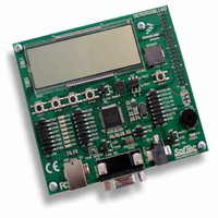
BOARD DEMO FOR 9S08LC60
Manufacturer
Freescale Semiconductor
Type
MCUr
Datasheets
1.DEMO9S08LC60.pdf
(360 pages)
2.DEMO9S08LC60.pdf
(32 pages)
3.DEMO9S08LC60.pdf
(2 pages)
Specifications of DEMO9S08LC60
Contents
Evaluation Board
Processor To Be Evaluated
MC9S08LC60
Interface Type
RS-232, USB
Silicon Manufacturer
Freescale
Core Architecture
HCS08
Core Sub-architecture
HCS08
Silicon Core Number
MC9S08
Silicon Family Name
S08LC
Rohs Compliant
Yes
For Use With/related Products
MC9S08LC60
Lead Free Status / RoHS Status
Lead free / RoHS Compliant


Chapter 6 Parallel Input/Output
The data direction control bit (PTxDDn) determines whether the output buffer for the associated pin is
enabled, and also controls the source for port data register reads. The input buffer for the associated pin is
always enabled unless the pin is enabled as an analog function or is an output-only pin.
When a shared digital function is enabled for a pin, the output buffer is controlled by the shared function.
However, the data direction register bit will continue to control the source for reads of the port data register.
When a shared analog function is enabled for a pin, both the input and output buffers are disabled. A value
of 0 is read for any port data bit where the bit is an input (PTxDDn = 0) and the input buffer is disabled.
In general, whenever a pin is shared with both an alternate digital function and an analog function, the
analog function has priority such that if both the digital and analog functions are enabled, the analog
function controls the pin.
It is a good programming practice to write to the port data register before changing the direction of a port
pin to become an output. This ensures that the pin will not be driven momentarily with an old data value
that happened to be in the port data register.
Associated with the parallel I/O ports is a set of registers located in the high page register space that operate
independently of the parallel I/O registers. These registers are used to control pullups, slew rate, and drive
strength for the pins. See
82
PORT READ
DATA
BUSCLK
Section 6.2.1, “Port A Registers
MC9S08LC60 Series Data Sheet: Technical Data, Rev. 4
PTxDDn
D
D
PTxDn
Figure 6-1. Parallel I/O Block Diagram
Q
Q
1
0
for more information.
SYNCHRONIZER
OUTPUT ENABLE
OUTPUT DATA
Freescale Semiconductor
INPUT DATA
Related parts for DEMO9S08LC60
Image
Part Number
Description
Manufacturer
Datasheet
Request
R

Part Number:
Description:
Manufacturer:
Freescale Semiconductor, Inc
Datasheet:
Part Number:
Description:
Manufacturer:
Freescale Semiconductor, Inc
Datasheet:
Part Number:
Description:
Manufacturer:
Freescale Semiconductor, Inc
Datasheet:
Part Number:
Description:
Manufacturer:
Freescale Semiconductor, Inc
Datasheet:
Part Number:
Description:
Manufacturer:
Freescale Semiconductor, Inc
Datasheet:
Part Number:
Description:
Manufacturer:
Freescale Semiconductor, Inc
Datasheet:
Part Number:
Description:
Manufacturer:
Freescale Semiconductor, Inc
Datasheet:
Part Number:
Description:
Manufacturer:
Freescale Semiconductor, Inc
Datasheet:
Part Number:
Description:
Manufacturer:
Freescale Semiconductor, Inc
Datasheet:
Part Number:
Description:
Manufacturer:
Freescale Semiconductor, Inc
Datasheet:
Part Number:
Description:
Manufacturer:
Freescale Semiconductor, Inc
Datasheet:
Part Number:
Description:
Manufacturer:
Freescale Semiconductor, Inc
Datasheet:
Part Number:
Description:
Manufacturer:
Freescale Semiconductor, Inc
Datasheet:
Part Number:
Description:
Manufacturer:
Freescale Semiconductor, Inc
Datasheet:
Part Number:
Description:
Manufacturer:
Freescale Semiconductor, Inc
Datasheet: