DEMO9S08LC60 Freescale Semiconductor, DEMO9S08LC60 Datasheet - Page 42
DEMO9S08LC60
Manufacturer Part Number
DEMO9S08LC60
Description
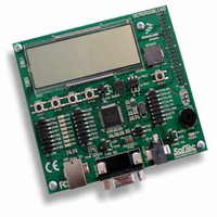
BOARD DEMO FOR 9S08LC60
Manufacturer
Freescale Semiconductor
Type
MCUr
Datasheets
1.DEMO9S08LC60.pdf
(360 pages)
2.DEMO9S08LC60.pdf
(32 pages)
3.DEMO9S08LC60.pdf
(2 pages)
Specifications of DEMO9S08LC60
Contents
Evaluation Board
Processor To Be Evaluated
MC9S08LC60
Interface Type
RS-232, USB
Silicon Manufacturer
Freescale
Core Architecture
HCS08
Core Sub-architecture
HCS08
Silicon Core Number
MC9S08
Silicon Family Name
S08LC
Rohs Compliant
Yes
For Use With/related Products
MC9S08LC60
Lead Free Status / RoHS Status
Lead free / RoHS Compliant


Chapter 4 Memory
4.2
The registers in the MC9S08LC60 Series are divided into these three groups:
Direct-page registers can be accessed with efficient direct addressing mode instructions. Bit manipulation
instructions can be used to access any bit in any direct-page register.
user-accessible direct-page registers and control bits.
The direct page registers in
requires the lower byte of the address. Because of this, the lower byte of the address in column one is
shown in bold text. In
Table
from the bit names to the right. Cells that are not associated with named bits are shaded. A shaded cell with
a 0 indicates this unused bit always reads as a 0. Shaded cells with dashes indicate unused or reserved bit
locations that could read as 1s or 0s.
42
•
•
•
4-2,
Direct-page registers are located in the first 128 locations in the memory map, so they are
accessible with efficient direct addressing mode instructions.
High-page registers are used much less often, so they are located above 0x1800 in the memory
map. This leaves more room in the direct page for more frequently used registers and variables.
The nonvolatile register area consists of a block of 16 locations in FLASH memory at
0xFFB0–0xFFBF.
Nonvolatile register locations include:
— NVPROT and NVOPT are loaded into working registers at reset
— An 8-byte backdoor comparison key which optionally allows a user to gain controlled access
Because the nonvolatile register locations are FLASH memory, they must be erased and
programmed like other FLASH memory locations.
Register Addresses and Bit Assignments
Table
to secure memory
4-3, and
Table 4-3
Table
Table 4-2
MC9S08LC60 Series Data Sheet: Technical Data, Rev. 4
4-4, the register names in column two are shown in bold to set them apart
and
Table 4-4
can use the more efficient direct addressing mode which only
the whole address in column one is shown in bold. In
Table 4-2
is a summary of all
Freescale Semiconductor
Related parts for DEMO9S08LC60
Image
Part Number
Description
Manufacturer
Datasheet
Request
R

Part Number:
Description:
Manufacturer:
Freescale Semiconductor, Inc
Datasheet:
Part Number:
Description:
Manufacturer:
Freescale Semiconductor, Inc
Datasheet:
Part Number:
Description:
Manufacturer:
Freescale Semiconductor, Inc
Datasheet:
Part Number:
Description:
Manufacturer:
Freescale Semiconductor, Inc
Datasheet:
Part Number:
Description:
Manufacturer:
Freescale Semiconductor, Inc
Datasheet:
Part Number:
Description:
Manufacturer:
Freescale Semiconductor, Inc
Datasheet:
Part Number:
Description:
Manufacturer:
Freescale Semiconductor, Inc
Datasheet:
Part Number:
Description:
Manufacturer:
Freescale Semiconductor, Inc
Datasheet:
Part Number:
Description:
Manufacturer:
Freescale Semiconductor, Inc
Datasheet:
Part Number:
Description:
Manufacturer:
Freescale Semiconductor, Inc
Datasheet:
Part Number:
Description:
Manufacturer:
Freescale Semiconductor, Inc
Datasheet:
Part Number:
Description:
Manufacturer:
Freescale Semiconductor, Inc
Datasheet:
Part Number:
Description:
Manufacturer:
Freescale Semiconductor, Inc
Datasheet:
Part Number:
Description:
Manufacturer:
Freescale Semiconductor, Inc
Datasheet:
Part Number:
Description:
Manufacturer:
Freescale Semiconductor, Inc
Datasheet: