DEMO9S08LC60 Freescale Semiconductor, DEMO9S08LC60 Datasheet - Page 81
DEMO9S08LC60
Manufacturer Part Number
DEMO9S08LC60
Description
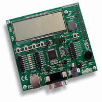
BOARD DEMO FOR 9S08LC60
Manufacturer
Freescale Semiconductor
Type
MCUr
Datasheets
1.DEMO9S08LC60.pdf
(360 pages)
2.DEMO9S08LC60.pdf
(32 pages)
3.DEMO9S08LC60.pdf
(2 pages)
Specifications of DEMO9S08LC60
Contents
Evaluation Board
Processor To Be Evaluated
MC9S08LC60
Interface Type
RS-232, USB
Silicon Manufacturer
Freescale
Core Architecture
HCS08
Core Sub-architecture
HCS08
Silicon Core Number
MC9S08
Silicon Family Name
S08LC
Rohs Compliant
Yes
For Use With/related Products
MC9S08LC60
Lead Free Status / RoHS Status
Lead free / RoHS Compliant


Chapter 6
Parallel Input/Output
This section explains software controls related to parallel input/output (I/O). The MC9S08LC60 Series has
three I/O ports which include a total of up to 24 general-purpose I/O pins (pin availability depends on
device and package option, see
information about the logic and hardware aspects of these pins.
Many of these pins are shared with on-chip peripherals such as timer systems, SPI, SCI, IIC, external
interrupts, or keyboard interrupts as shown in Table 2-1. The peripheral modules have priority over the I/Os
so that when a peripheral is enabled, the I/O functions associated with the shared pins are disabled. After
reset, the shared peripheral functions are disabled so that the pins are controlled by the I/O. All of the I/Os
are configured as inputs (PTxDDn = 0) with pullup devices disabled (PTxPEn = 0), except for output-only
pin PTC6 which defaults to BKGD/MS pin and PTB2 which defaults to the RESET function.
When these other modules are not controlling the port pins, they revert to general-purpose I/O control. As
a general-purpose I/O control, a port data bit provides access to input (read) and output (write) data, a data
direction bit controls the direction of the pin, and a pullup enable bit enables an internal pullup device
(provided the pin is configured as an input), and a slew rate control bit controls the rise and fall times of
the pins.
Reading and writing of parallel I/Os is performed through the port data registers. The direction, either input
or output, is controlled through the port data direction registers. The parallel I/O port function for an
individual pin is illustrated in the block diagram shown in
Freescale Semiconductor
Not all general-purpose I/O pins are available on all packages. To avoid
extra current drain from floating input pins, the user’s reset initialization
routine in the application program should either enable on-chip pullup
devices or change the direction of unconnected pins to outputs so the pins
do not float.
MC9S08LC60 Series Data Sheet: Technical Data, Rev. 4
Table 1-2
for details). See
NOTE
Chapter 2, “Pins and
Figure
6-1.
Connections,” for more
81
Related parts for DEMO9S08LC60
Image
Part Number
Description
Manufacturer
Datasheet
Request
R

Part Number:
Description:
Manufacturer:
Freescale Semiconductor, Inc
Datasheet:
Part Number:
Description:
Manufacturer:
Freescale Semiconductor, Inc
Datasheet:
Part Number:
Description:
Manufacturer:
Freescale Semiconductor, Inc
Datasheet:
Part Number:
Description:
Manufacturer:
Freescale Semiconductor, Inc
Datasheet:
Part Number:
Description:
Manufacturer:
Freescale Semiconductor, Inc
Datasheet:
Part Number:
Description:
Manufacturer:
Freescale Semiconductor, Inc
Datasheet:
Part Number:
Description:
Manufacturer:
Freescale Semiconductor, Inc
Datasheet:
Part Number:
Description:
Manufacturer:
Freescale Semiconductor, Inc
Datasheet:
Part Number:
Description:
Manufacturer:
Freescale Semiconductor, Inc
Datasheet:
Part Number:
Description:
Manufacturer:
Freescale Semiconductor, Inc
Datasheet:
Part Number:
Description:
Manufacturer:
Freescale Semiconductor, Inc
Datasheet:
Part Number:
Description:
Manufacturer:
Freescale Semiconductor, Inc
Datasheet:
Part Number:
Description:
Manufacturer:
Freescale Semiconductor, Inc
Datasheet:
Part Number:
Description:
Manufacturer:
Freescale Semiconductor, Inc
Datasheet:
Part Number:
Description:
Manufacturer:
Freescale Semiconductor, Inc
Datasheet: