DEMO9S08LC60 Freescale Semiconductor, DEMO9S08LC60 Datasheet - Page 49
DEMO9S08LC60
Manufacturer Part Number
DEMO9S08LC60
Description
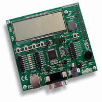
BOARD DEMO FOR 9S08LC60
Manufacturer
Freescale Semiconductor
Type
MCUr
Datasheets
1.DEMO9S08LC60.pdf
(360 pages)
2.DEMO9S08LC60.pdf
(32 pages)
3.DEMO9S08LC60.pdf
(2 pages)
Specifications of DEMO9S08LC60
Contents
Evaluation Board
Processor To Be Evaluated
MC9S08LC60
Interface Type
RS-232, USB
Silicon Manufacturer
Freescale
Core Architecture
HCS08
Core Sub-architecture
HCS08
Silicon Core Number
MC9S08
Silicon Family Name
S08LC
Rohs Compliant
Yes
For Use With/related Products
MC9S08LC60
Lead Free Status / RoHS Status
Lead free / RoHS Compliant


4.4.1
Features of the FLASH memory include:
4.4.2
Before any program or erase command can be accepted, the FLASH clock divider register (FCDIV) must
be written to set the internal clock for the FLASH module to a frequency (f
200 kHz (see
once, so normally this write is done during reset initialization. FCDIV cannot be written if the access error
flag, FACCERR in FSTAT, is set. The user must ensure that FACCERR is not set before writing to the
FCDIV register. One period of the resulting clock (1/f
program and erase pulses. An integer number of these timing pulses is used by the command processor to
complete a program or erase command.
Table 4-5
of FCLK (f
of cycles of FCLK and as an absolute time for the case where t
shown include overhead for the command state machine and enabling and disabling of program and erase
voltages.
Freescale Semiconductor
•
•
•
•
•
•
•
•
FLASH Size
— MC9S08LC60 — 63,232 bytes (28,464 bytes in Flash B, 32,768 bytes in Flash A)
— MC9S08LC36 — 36,864 bytes (12,288 bytes in Flash B, 24,576 bytes in Flash A)
Single power supply program and erase
Command interface for fast program and erase operation
Up to 100,000 program/erase cycles at typical voltage and temperature
Flexible block protection
Security feature for FLASH and RAM
Auto power-down for low-frequency read accesses to minimize run I
FLASH read/program/erase over full operating voltage or temperature
shows program and erase times. The bus clock frequency and FCDIV determine the frequency
Features
Program and Erase Times
FCLK
1
Section 4.6.1, “FLASH Clock Divider Register
Byte program
Byte program (burst)
Page erase
Mass erase
Excluding start/end overhead
). The time for one cycle of FCLK is t
Parameter
MC9S08LC60 Series Data Sheet: Technical Data, Rev. 4
Table 4-5. Program and Erase Times
Cycles of FCLK
20,000
4000
9
4
FCLK
FCLK
) is used by the command processor to time
= 1/f
(FCDIV)). This register can be written only
FCLK
FCLK
Time if FCLK = 200 kHz
= 5 μs. Program and erase times
. The times are shown as a number
FCLK
100 ms
20 μs
20 ms
DD
45 μs
) between 150 kHz and
1
Chapter 4 Memory
49
Related parts for DEMO9S08LC60
Image
Part Number
Description
Manufacturer
Datasheet
Request
R

Part Number:
Description:
Manufacturer:
Freescale Semiconductor, Inc
Datasheet:
Part Number:
Description:
Manufacturer:
Freescale Semiconductor, Inc
Datasheet:
Part Number:
Description:
Manufacturer:
Freescale Semiconductor, Inc
Datasheet:
Part Number:
Description:
Manufacturer:
Freescale Semiconductor, Inc
Datasheet:
Part Number:
Description:
Manufacturer:
Freescale Semiconductor, Inc
Datasheet:
Part Number:
Description:
Manufacturer:
Freescale Semiconductor, Inc
Datasheet:
Part Number:
Description:
Manufacturer:
Freescale Semiconductor, Inc
Datasheet:
Part Number:
Description:
Manufacturer:
Freescale Semiconductor, Inc
Datasheet:
Part Number:
Description:
Manufacturer:
Freescale Semiconductor, Inc
Datasheet:
Part Number:
Description:
Manufacturer:
Freescale Semiconductor, Inc
Datasheet:
Part Number:
Description:
Manufacturer:
Freescale Semiconductor, Inc
Datasheet:
Part Number:
Description:
Manufacturer:
Freescale Semiconductor, Inc
Datasheet:
Part Number:
Description:
Manufacturer:
Freescale Semiconductor, Inc
Datasheet:
Part Number:
Description:
Manufacturer:
Freescale Semiconductor, Inc
Datasheet:
Part Number:
Description:
Manufacturer:
Freescale Semiconductor, Inc
Datasheet: