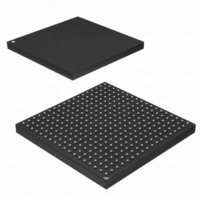
AT91SAM9G45-CU-999 Atmel, AT91SAM9G45-CU-999 Datasheet - Page 1204

AT91SAM9G45-CU-999
Manufacturer Part Number
AT91SAM9G45-CU-999
Description
IC MCU ARM9 APMC 324TFBGA
Manufacturer
Atmel
Series
AT91SAMr
Datasheet
1.AT91SAM9G45-EKES.pdf
(1218 pages)
Specifications of AT91SAM9G45-CU-999
Core Processor
ARM9
Core Size
16/32-Bit
Speed
400MHz
Connectivity
EBI/EMI, Ethernet, I²C, IrDA, MMC, SPI, SSC, UART/USART, USB
Peripherals
AC'97, DMA, I²S, LCD, POR, PWM, WDT
Number Of I /o
160
Program Memory Size
64KB (64K x 8)
Program Memory Type
ROM
Ram Size
128K x 8
Voltage - Supply (vcc/vdd)
0.9 V ~ 1.1 V
Data Converters
A/D 8x10b
Oscillator Type
Internal
Operating Temperature
-40°C ~ 85°C
Package / Case
324-TFBGA
Lead Free Status / RoHS Status
Lead free / RoHS Compliant
Eeprom Size
-
Lead Free Status / Rohs Status
Supplier Unconfirmed
Available stocks
Company
Part Number
Manufacturer
Quantity
Price
- Current page: 1204 of 1218
- Download datasheet (19Mb)
1204
Doc. Rev
6438D
Doc. Rev
6438C
Doc. Rev
6438B
AT91SAM9G45
Comments
LCD Controller (LCDC):
Section 45.12.12 “LCD Timing Configuration Register
written to 1’ added to VHDLY definition.
Parallel Input/Output Controller (PIO):
- DELAY Registers were addded in a
description added in a
-
Register”and
In
Clear Output Data”
All ‘slewrate’ changed into ‘drive’.
All ‘IO’ changed into ‘I/O’.
All
Any extra ‘Controller’ or ‘Controller PIO’ removed.
Static Memory Controller (SMC):
Table 21-5 removed from
21-8
USB Host Port:
Section 37. “USB High Speed Host Port (UHPHS)”
Comments
Introduction:
Section 3. “Signal Description”
concerning NRST configuration.
Section 4. “Package and
Boot Program:
Section 11.5.2.1 “Supported External Crystal/External
RSTC:
Section 12.5 “Reset Controller (RSTC) User Interface” Table 12-1
0x0000 0001.
Comments
DDRSDRC:
Section 22.7.3 “DDRSDRC Configuration
Section 22.7.9 “DDRSDRC DLL Register”
removed from register.
“Write Protected Registers”
Section 30.6.11 “PIO Clear Output Data
Section 30.6 “Parallel Input/Output Controller (PIO) User Interface”
instead.
Section 30.6.32 “PIO Write Protect Status
Section 30.6.30 “PIO I/O Delay
Pinout”,
Section 21.8.6 “Reset Values of Timing
description added, together with
,
Table
Table 4-1
Section 30.4.12 “Programmable I/O Delays”
3-1, in
Register”, bit named ENRDM removed from register.
bits named, SDCOVF, SDCUDF, SDERF, SDVAL, SDCVAL
Register”, “P0-P31: Set Output Data” changed into “P0-P31:
updated.
“Reset/Test”
, HS (High Speed) was added to the title.
1”, ‘-’ replaced by ‘1’ for bit 31, and ‘Bit 31 must be
Clocks”, ...”supports 12 MHz”...
Register”.
Register”.
description, NRST pin updated with note
Section 30.6.31 “PIO Write Protect Mode
Parameters”. Cross-referenced
Mode register backup reset value is
headers now start with ‘PIO’ only.
and associated register
Table
6438F–ATARM–21-Jun-10
Change
Request
Ref.
6685
6715
6742
6644
Change
Request
Ref.
6600
6639
6598
6639
Change
Request
Ref.
6606
Related parts for AT91SAM9G45-CU-999
Image
Part Number
Description
Manufacturer
Datasheet
Request
R

Part Number:
Description:
KIT EVAL FOR AT91SAM9G45
Manufacturer:
Atmel
Datasheet:

Part Number:
Description:
MCU ARM9 324-TFBGA
Manufacturer:
Atmel
Datasheet:

Part Number:
Description:
At91 Arm Thumb-based Microcontrollers
Manufacturer:
ATMEL Corporation
Datasheet:

Part Number:
Description:
MCU, MPU & DSP Development Tools KICKSTART KIT FOR AT91SAM9 PLUS
Manufacturer:
IAR Systems

Part Number:
Description:
DEV KIT FOR AVR/AVR32
Manufacturer:
Atmel
Datasheet:

Part Number:
Description:
INTERVAL AND WIPE/WASH WIPER CONTROL IC WITH DELAY
Manufacturer:
ATMEL Corporation
Datasheet:

Part Number:
Description:
Low-Voltage Voice-Switched IC for Hands-Free Operation
Manufacturer:
ATMEL Corporation
Datasheet:

Part Number:
Description:
MONOLITHIC INTEGRATED FEATUREPHONE CIRCUIT
Manufacturer:
ATMEL Corporation
Datasheet:

Part Number:
Description:
AM-FM Receiver IC U4255BM-M
Manufacturer:
ATMEL Corporation
Datasheet:

Part Number:
Description:
Monolithic Integrated Feature Phone Circuit
Manufacturer:
ATMEL Corporation
Datasheet:

Part Number:
Description:
Multistandard Video-IF and Quasi Parallel Sound Processing
Manufacturer:
ATMEL Corporation
Datasheet:

Part Number:
Description:
High-performance EE PLD
Manufacturer:
ATMEL Corporation
Datasheet:


