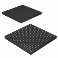
AT91SAM9G45-CU-999 Atmel, AT91SAM9G45-CU-999 Datasheet - Page 685

AT91SAM9G45-CU-999
Manufacturer Part Number
AT91SAM9G45-CU-999
Description
IC MCU ARM9 APMC 324TFBGA
Manufacturer
Atmel
Series
AT91SAMr
Datasheet
1.AT91SAM9G45-EKES.pdf
(1218 pages)
Specifications of AT91SAM9G45-CU-999
Core Processor
ARM9
Core Size
16/32-Bit
Speed
400MHz
Connectivity
EBI/EMI, Ethernet, I²C, IrDA, MMC, SPI, SSC, UART/USART, USB
Peripherals
AC'97, DMA, I²S, LCD, POR, PWM, WDT
Number Of I /o
160
Program Memory Size
64KB (64K x 8)
Program Memory Type
ROM
Ram Size
128K x 8
Voltage - Supply (vcc/vdd)
0.9 V ~ 1.1 V
Data Converters
A/D 8x10b
Oscillator Type
Internal
Operating Temperature
-40°C ~ 85°C
Package / Case
324-TFBGA
Lead Free Status / RoHS Status
Lead free / RoHS Compliant
Eeprom Size
-
Lead Free Status / Rohs Status
Supplier Unconfirmed
Available stocks
Company
Part Number
Manufacturer
Quantity
Price
- Current page: 685 of 1218
- Download datasheet (19Mb)
34.9.4
Name:
Addresses:
Access:
• DATLEN: Data Length
0 = Forbidden value (1-bit data length not supported).
Any other value: The bit stream contains DATLEN + 1 data bits. Moreover, it defines the transfer size performed by the
PDC assigned to the Receiver. If DATLEN is lower or equal to 7, data transfers are in bytes. If DATLEN is between 8 and
15 (included), half-words are transferred, and for any other value, 32-bit words are transferred.
• LOOP: Loop Mode
0 = Normal operating mode.
1 = RD is driven by TD, RF is driven by TF and TK drives RK.
• MSBF: Most Significant Bit First
0 = The lowest significant bit of the data register is sampled first in the bit stream.
1 = The most significant bit of the data register is sampled first in the bit stream.
• DATNB: Data Number per Frame
This field defines the number of data words to be received after each transfer start, which is equal to (DATNB + 1).
• FSLEN: Receive Frame Sync Length
This field defines the number of bits sampled and stored in the Receive Sync Data Register. When this mode is selected by
the START field in the Receive Clock Mode Register, it also determines the length of the sampled data to be compared to
the Compare 0 or Compare 1 register.
This field is used with FSLEN_EXT to determine the pulse length of the Receive Frame Sync signal.
Pulse length is equal to FSLEN + (FSLEN_EXT * 16) + 1 Receive Clock periods.
6438F–ATARM–21-Jun-10
FSLEN_EXT
MSBF
31
23
15
–
–
7
SSC Receive Frame Mode Register
FSLEN_EXT
30
22
14
SSC_RFMR
0xFFF9C014 (0), 0xFFFA0014 (1)
Read-write
–
6
–
FSLEN_EXT
LOOP
FSOS
29
21
13
–
5
FSLEN_EXT
28
20
12
–
4
27
19
11
–
3
DATLEN
26
18
10
–
2
FSLEN
DATNB
AT91SAM9G45
25
17
–
9
1
FSEDGE
24
16
8
0
685
Related parts for AT91SAM9G45-CU-999
Image
Part Number
Description
Manufacturer
Datasheet
Request
R

Part Number:
Description:
KIT EVAL FOR AT91SAM9G45
Manufacturer:
Atmel
Datasheet:

Part Number:
Description:
MCU ARM9 324-TFBGA
Manufacturer:
Atmel
Datasheet:

Part Number:
Description:
At91 Arm Thumb-based Microcontrollers
Manufacturer:
ATMEL Corporation
Datasheet:

Part Number:
Description:
MCU, MPU & DSP Development Tools KICKSTART KIT FOR AT91SAM9 PLUS
Manufacturer:
IAR Systems

Part Number:
Description:
DEV KIT FOR AVR/AVR32
Manufacturer:
Atmel
Datasheet:

Part Number:
Description:
INTERVAL AND WIPE/WASH WIPER CONTROL IC WITH DELAY
Manufacturer:
ATMEL Corporation
Datasheet:

Part Number:
Description:
Low-Voltage Voice-Switched IC for Hands-Free Operation
Manufacturer:
ATMEL Corporation
Datasheet:

Part Number:
Description:
MONOLITHIC INTEGRATED FEATUREPHONE CIRCUIT
Manufacturer:
ATMEL Corporation
Datasheet:

Part Number:
Description:
AM-FM Receiver IC U4255BM-M
Manufacturer:
ATMEL Corporation
Datasheet:

Part Number:
Description:
Monolithic Integrated Feature Phone Circuit
Manufacturer:
ATMEL Corporation
Datasheet:

Part Number:
Description:
Multistandard Video-IF and Quasi Parallel Sound Processing
Manufacturer:
ATMEL Corporation
Datasheet:

Part Number:
Description:
High-performance EE PLD
Manufacturer:
ATMEL Corporation
Datasheet:


