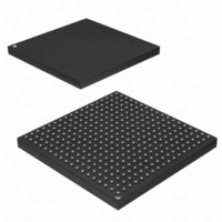
AT91SAM9G45-CU-999 Atmel, AT91SAM9G45-CU-999 Datasheet - Page 183

AT91SAM9G45-CU-999
Manufacturer Part Number
AT91SAM9G45-CU-999
Description
IC MCU ARM9 APMC 324TFBGA
Manufacturer
Atmel
Series
AT91SAMr
Datasheet
1.AT91SAM9G45-EKES.pdf
(1218 pages)
Specifications of AT91SAM9G45-CU-999
Core Processor
ARM9
Core Size
16/32-Bit
Speed
400MHz
Connectivity
EBI/EMI, Ethernet, I²C, IrDA, MMC, SPI, SSC, UART/USART, USB
Peripherals
AC'97, DMA, I²S, LCD, POR, PWM, WDT
Number Of I /o
160
Program Memory Size
64KB (64K x 8)
Program Memory Type
ROM
Ram Size
128K x 8
Voltage - Supply (vcc/vdd)
0.9 V ~ 1.1 V
Data Converters
A/D 8x10b
Oscillator Type
Internal
Operating Temperature
-40°C ~ 85°C
Package / Case
324-TFBGA
Lead Free Status / RoHS Status
Lead free / RoHS Compliant
Eeprom Size
-
Lead Free Status / Rohs Status
Supplier Unconfirmed
Available stocks
Company
Part Number
Manufacturer
Quantity
Price
- Current page: 183 of 1218
- Download datasheet (19Mb)
20.2.9
6438F–ATARM–21-Jun-10
Programmable I/O Lines Power Supplies and Drive Levels
The power supply pin VDDIOM1 accepts two voltage ranges. This allows the device to reach its
maximum speed either out of 1.8V or 3.3V external memories.
The maximum speed is 133 MHz on the SDCK pin and #SDCK signals loaded with 10 pF. The
load on data/address and control signals are 30 pF for power supply at 1.8V and 50 pF for power
supply at 3.3V. The data lines frequency reaches 133 MHz in DDR2 mode. The other signals
(control and address) do not go over 66 MHz.
The EBI I/Os accept two drive levels, HIGH and LOW. This allows to avoid overshoots and give
the best performance according to the bus load and external memories. Refer to the EBI Chip
Select Assignment Register for more details.
The voltage ranges and the drive level are determined by programming EBI_DRIVE field in the
Chip Configuration registers located in the Matrix User Interface.
At reset the selected default drive level is High.
At reset, the selected voltage defaults to 3.3V typical and power supply pins can accept either
1.8V or 3.3V. The user must make sure to program the EBI voltage range before getting the
device out of its Slow Clock Mode. The user must make sure to program the EBI voltage range
before getting the device out of its Slow Clock Mode.
• Assign the EBI CS4 and/or EBI_CS5 to the CompactFlash Slot 0 and/or Slot 1 by setting the
• The address line A21 is to select Alternate True IDE (A21=1) or True IDE (A21=0) modes.
• A21, CFRNW, CFS0, CFCS1, CFCE1 and CFCE2 signals are multiplexed with PIO lines and
• Configure a PIO line as an output for CFRST and two others as an input for CFIRQ and
• Configure SMC CS4 and/or SMC_CS5 (for Slot 0 or 1) Setup, Pulse, Cycle and Mode
bit EBI_CS4A and/or EBI_CS5A in the EBI Chip Select Assignment Register located in the
bus matrix memory space.
thus the dedicated PIOs must be programmed in peripheral mode in the PIO controller.
CARD DETECT functions respectively.
accordingly to CompactFlash timings and system bus frequency.
AT91SAM9G45
183
Related parts for AT91SAM9G45-CU-999
Image
Part Number
Description
Manufacturer
Datasheet
Request
R

Part Number:
Description:
KIT EVAL FOR AT91SAM9G45
Manufacturer:
Atmel
Datasheet:

Part Number:
Description:
MCU ARM9 324-TFBGA
Manufacturer:
Atmel
Datasheet:

Part Number:
Description:
At91 Arm Thumb-based Microcontrollers
Manufacturer:
ATMEL Corporation
Datasheet:

Part Number:
Description:
MCU, MPU & DSP Development Tools KICKSTART KIT FOR AT91SAM9 PLUS
Manufacturer:
IAR Systems

Part Number:
Description:
DEV KIT FOR AVR/AVR32
Manufacturer:
Atmel
Datasheet:

Part Number:
Description:
INTERVAL AND WIPE/WASH WIPER CONTROL IC WITH DELAY
Manufacturer:
ATMEL Corporation
Datasheet:

Part Number:
Description:
Low-Voltage Voice-Switched IC for Hands-Free Operation
Manufacturer:
ATMEL Corporation
Datasheet:

Part Number:
Description:
MONOLITHIC INTEGRATED FEATUREPHONE CIRCUIT
Manufacturer:
ATMEL Corporation
Datasheet:

Part Number:
Description:
AM-FM Receiver IC U4255BM-M
Manufacturer:
ATMEL Corporation
Datasheet:

Part Number:
Description:
Monolithic Integrated Feature Phone Circuit
Manufacturer:
ATMEL Corporation
Datasheet:

Part Number:
Description:
Multistandard Video-IF and Quasi Parallel Sound Processing
Manufacturer:
ATMEL Corporation
Datasheet:

Part Number:
Description:
High-performance EE PLD
Manufacturer:
ATMEL Corporation
Datasheet:


