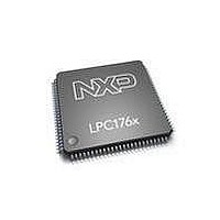
LPC1759FBD80,551 NXP Semiconductors, LPC1759FBD80,551 Datasheet - Page 633

LPC1759FBD80,551
Manufacturer Part Number
LPC1759FBD80,551
Description
IC ARM CORTEX MCU 512K 80-LQFP
Manufacturer
NXP Semiconductors
Series
LPC17xxr
Datasheets
1.LPC1751FBD80551.pdf
(74 pages)
2.LPC1767FBD100551.pdf
(2 pages)
3.LPC1767FBD100551.pdf
(840 pages)
Specifications of LPC1759FBD80,551
Program Memory Type
FLASH
Program Memory Size
512KB (512K x 8)
Package / Case
80-LQFP
Core Processor
ARM® Cortex-M3™
Core Size
32-Bit
Speed
120MHz
Connectivity
CAN, I²C, IrDA, Microwire, SPI, SSI, SSP, UART/USART, USB OTG
Peripherals
Brown-out Detect/Reset, DMA, I²S, Motor Control PWM, POR, PWM, WDT
Number Of I /o
52
Ram Size
64K x 8
Voltage - Supply (vcc/vdd)
2.4 V ~ 3.6 V
Data Converters
A/D 6x12b, D/A 1x10b
Oscillator Type
Internal
Operating Temperature
-40°C ~ 85°C
Processor Series
LPC17
Core
ARM Cortex M3
Data Bus Width
32 bit
Data Ram Size
64 KB
Interface Type
Ethernet, USB, OTG, CAN
Maximum Clock Frequency
120 MHz
Number Of Programmable I/os
52
Number Of Timers
4
Operating Supply Voltage
3.3 V
Maximum Operating Temperature
+ 85 C
Mounting Style
SMD/SMT
3rd Party Development Tools
MDK-ARM, RL-ARM, ULINK2
Minimum Operating Temperature
- 40 C
On-chip Adc
12 bit, 6 Channel
On-chip Dac
10 bit
Package
80LQFP
Device Core
ARM Cortex M3
Family Name
LPC17xx
Maximum Speed
120 MHz
Lead Free Status / RoHS Status
Lead free / RoHS Compliant
For Use With
622-1005 - USB IN-CIRCUIT PROG ARM7 LPC2K
Eeprom Size
-
Lead Free Status / Rohs Status
Lead free / RoHS Compliant
Other names
568-4968
935290523551
935290523551
Available stocks
Company
Part Number
Manufacturer
Quantity
Price
Company:
Part Number:
LPC1759FBD80,551
Manufacturer:
LT
Quantity:
375
Company:
Part Number:
LPC1759FBD80,551
Manufacturer:
NXP Semiconductors
Quantity:
10 000
Part Number:
LPC1759FBD80,551
Manufacturer:
NXP/恩智浦
Quantity:
20 000
- Current page: 633 of 840
- Download datasheet (6Mb)
NXP Semiconductors
UM10360
User manual
32.8.2 Copy RAM to Flash
Table 589. IAP Prepare sector(s) for write operation command
Table 590. IAP Copy RAM to Flash command
Command
Input
Return Code
Result
Description
Command
Input
Return Code
Result
Description
Prepare sector(s) for write operation
Command code: 5010
Param0: Start Sector Number
Param1: End Sector Number (should be greater than or equal to start sector
number).
CMD_SUCCESS |
BUSY |
INVALID_SECTOR
None
This command must be executed before executing "Copy RAM to Flash" or
"Erase Sector(s)" command. Successful execution of the "Copy RAM to Flash" or
"Erase Sector(s)" command causes relevant sectors to be protected again. To
prepare a single sector use the same "Start" and "End" sector numbers.
Copy RAM to Flash
Command code: 5110
Param0(DST): Destination flash address where data bytes are to be written. This
address should be a 256 byte boundary.
Param1(SRC): Source RAM address from which data bytes are to be read. This
address should be a word boundary.
Param2: Number of bytes to be written. Should be 256 | 512 | 1024 | 4096.
Param3: CPU Clock Frequency (CCLK) in kHz.
CMD_SUCCESS |
SRC_ADDR_ERROR (Address not a word boundary) |
DST_ADDR_ERROR (Address not on correct boundary) |
SRC_ADDR_NOT_MAPPED |
DST_ADDR_NOT_MAPPED |
COUNT_ERROR (Byte count is not 256 | 512 | 1024 | 4096) |
SECTOR_NOT_PREPARED_FOR_WRITE_OPERATION |
BUSY |
None
This command is used to program the flash memory. The affected sectors should
be prepared first by calling "Prepare Sector for Write Operation" command. The
affected sectors are automatically protected again once the copy command is
successfully executed.
All information provided in this document is subject to legal disclaimers.
Chapter 32: LPC17xx Flash memory interface and programming
Rev. 2 — 19 August 2010
UM10360
© NXP B.V. 2010. All rights reserved.
633 of 840
Related parts for LPC1759FBD80,551
Image
Part Number
Description
Manufacturer
Datasheet
Request
R
Part Number:
Description:
Lpc17xx Device Highlight
Manufacturer:
NXP Semiconductors
Datasheet:
Part Number:
Description:
NXP Semiconductors designed the LPC2420/2460 microcontroller around a 16-bit/32-bitARM7TDMI-S CPU core with real-time debug interfaces that include both JTAG andembedded trace
Manufacturer:
NXP Semiconductors
Datasheet:

Part Number:
Description:
NXP Semiconductors designed the LPC2458 microcontroller around a 16-bit/32-bitARM7TDMI-S CPU core with real-time debug interfaces that include both JTAG andembedded trace
Manufacturer:
NXP Semiconductors
Datasheet:
Part Number:
Description:
NXP Semiconductors designed the LPC2468 microcontroller around a 16-bit/32-bitARM7TDMI-S CPU core with real-time debug interfaces that include both JTAG andembedded trace
Manufacturer:
NXP Semiconductors
Datasheet:
Part Number:
Description:
NXP Semiconductors designed the LPC2470 microcontroller, powered by theARM7TDMI-S core, to be a highly integrated microcontroller for a wide range ofapplications that require advanced communications and high quality graphic displays
Manufacturer:
NXP Semiconductors
Datasheet:
Part Number:
Description:
NXP Semiconductors designed the LPC2478 microcontroller, powered by theARM7TDMI-S core, to be a highly integrated microcontroller for a wide range ofapplications that require advanced communications and high quality graphic displays
Manufacturer:
NXP Semiconductors
Datasheet:
Part Number:
Description:
The Philips Semiconductors XA (eXtended Architecture) family of 16-bit single-chip microcontrollers is powerful enough to easily handle the requirements of high performance embedded applications, yet inexpensive enough to compete in the market for hi
Manufacturer:
NXP Semiconductors
Datasheet:
Part Number:
Description:
The XA-S3 device is a member of Philips Semiconductors? XA(eXtended Architecture) family of high performance 16-bitsingle-chip microcontrollers
Manufacturer:
NXP Semiconductors
Datasheet:

Part Number:
Description:
The NXP BlueStreak LH75401/LH75411 family consists of two low-cost 16/32-bit System-on-Chip (SoC) devices
Manufacturer:
NXP Semiconductors
Datasheet:

Part Number:
Description:
The NXP LPC3130/3131 combine an 180 MHz ARM926EJ-S CPU core, high-speed USB2
Manufacturer:
NXP Semiconductors
Datasheet:

Part Number:
Description:
The NXP LPC3141 combine a 270 MHz ARM926EJ-S CPU core, High-speed USB 2
Manufacturer:
NXP Semiconductors

Part Number:
Description:
The NXP LPC3143 combine a 270 MHz ARM926EJ-S CPU core, High-speed USB 2
Manufacturer:
NXP Semiconductors

Part Number:
Description:
The NXP LPC3152 combines an 180 MHz ARM926EJ-S CPU core, High-speed USB 2
Manufacturer:
NXP Semiconductors

Part Number:
Description:
The NXP LPC3154 combines an 180 MHz ARM926EJ-S CPU core, High-speed USB 2
Manufacturer:
NXP Semiconductors


