Z8F16800144ZCOG Zilog, Z8F16800144ZCOG Datasheet - Page 277
Z8F16800144ZCOG
Manufacturer Part Number
Z8F16800144ZCOG
Description
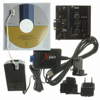
KIT DEV FOR Z8F642 MCU 44 PIN
Manufacturer
Zilog
Series
Z8 Encore!®r
Type
MCUr
Specifications of Z8F16800144ZCOG
Contents
Hardware, Software and Documentation
For Use With/related Products
Z8F642
For Use With
269-4661 - KIT ACC ETHERNET SMART CABLE
Lead Free Status / RoHS Status
Lead free / RoHS Compliant
Other names
269-4678


Table 137. Flash Page Select Register (FPS)
BITS
FIELD
RESET
R/W
ADDR
PS025011-1010
Flash Page Select Register
Flash Sector Protect Register
INFO_EN
R/W
7
0
001xxx = Program operation in progress.
010xxx = Page erase operation in progress.
100xxx = Mass erase operation in progress.
The Flash Page Select register (see
Flash Sector Protect Register. Unless the Flash controller is unlocked and written with
5EH, writes to this address target the Flash Page Select Register.
The register is used to select one of the Flash memory pages to be programmed or erased.
Each Flash Page contains 512 bytes of Flash memory. During a Page Erase operation, all
Flash memory having addresses with the most significant 7-bits given by FPS[6:0] are
chosen for program/erase operation.
INFO_EN—Information Area Enable
0 = Information Area is not selected
1 = Information Area is selected. The Information Area is mapped into the
PAGE—Page Select
This 7-bit field identifies the Flash memory page for Page Erase and page unlocking.
Program Memory Address[15:9] = PAGE[6:0]. For the Z8F2480 devices, the upper 1 bit
must always be 0. For the Z8F1680 devices, the upper 2 bits must always be 0. For the
Z8F0880 devices, the upper 3 bits must always be 0.
The Flash Sector Protect register is shared with the Flash Page Select Register. When the
Flash Control Register
this address targets the Flash Sector Protect Register. In all other cases, it targets the Flash
Page Select Register.
This register selects one of the eight available Flash memory sectors to be protected. The
reset state of each Sector Protect bit is an unprotected state. After a sector is protected by
Program Memory address space at addresses FE00H through FFFFH.
R/W
6
0
R/W
on page 261 is written with 73H followed by 5EH, the next write to
5
0
P R E L I M I N A R Y
R/W
Table 137
4
0
FF9H
PAGE
on page 263) shares address space with the
R/W
3
0
Z8 Encore! XP
R/W
2
0
Product Specification
R/W
1
0
®
F1680 Series
Flash Memory
R/W
0
0
263
Related parts for Z8F16800144ZCOG
Image
Part Number
Description
Manufacturer
Datasheet
Request
R

Part Number:
Description:
Communication Controllers, ZILOG INTELLIGENT PERIPHERAL CONTROLLER (ZIP)
Manufacturer:
Zilog, Inc.
Datasheet:

Part Number:
Description:
KIT DEV FOR Z8 ENCORE 16K TO 64K
Manufacturer:
Zilog
Datasheet:

Part Number:
Description:
KIT DEV Z8 ENCORE XP 28-PIN
Manufacturer:
Zilog
Datasheet:

Part Number:
Description:
DEV KIT FOR Z8 ENCORE 8K/4K
Manufacturer:
Zilog
Datasheet:

Part Number:
Description:
KIT DEV Z8 ENCORE XP 28-PIN
Manufacturer:
Zilog
Datasheet:

Part Number:
Description:
DEV KIT FOR Z8 ENCORE 4K TO 8K
Manufacturer:
Zilog
Datasheet:
Part Number:
Description:
CMOS Z8 microcontroller. ROM 16 Kbytes, RAM 256 bytes, speed 16 MHz, 32 lines I/O, 3.0V to 5.5V
Manufacturer:
Zilog, Inc.
Datasheet:
Part Number:
Description:
Low-cost microcontroller. 512 bytes ROM, 61 bytes RAM, 8 MHz
Manufacturer:
Zilog, Inc.
Datasheet:
Part Number:
Description:
Z8 4K OTP Microcontroller
Manufacturer:
Zilog, Inc.
Datasheet:
Part Number:
Description:
CMOS SUPER8 ROMLESS MCU
Manufacturer:
Zilog, Inc.
Datasheet:
Part Number:
Description:
SL1866 CMOSZ8 OTP Microcontroller
Manufacturer:
Zilog, Inc.
Datasheet:
Part Number:
Description:
SL1866 CMOSZ8 OTP Microcontroller
Manufacturer:
Zilog, Inc.
Datasheet:
Part Number:
Description:
OTP (KB) = 1, RAM = 125, Speed = 12, I/O = 14, 8-bit Timers = 2, Comm Interfaces Other Features = Por, LV Protect, Voltage = 4.5-5.5V
Manufacturer:
Zilog, Inc.
Datasheet:
Part Number:
Description:
Manufacturer:
Zilog, Inc.
Datasheet: