Z8F16800144ZCOG Zilog, Z8F16800144ZCOG Datasheet - Page 39
Z8F16800144ZCOG
Manufacturer Part Number
Z8F16800144ZCOG
Description
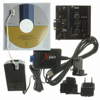
KIT DEV FOR Z8F642 MCU 44 PIN
Manufacturer
Zilog
Series
Z8 Encore!®r
Type
MCUr
Specifications of Z8F16800144ZCOG
Contents
Hardware, Software and Documentation
For Use With/related Products
Z8F642
For Use With
269-4661 - KIT ACC ETHERNET SMART CABLE
Lead Free Status / RoHS Status
Lead free / RoHS Compliant
Other names
269-4678


Table 7. Register File Address Map
Register Map
Address (Hex)
General Purpose RAM
Z8F2480 Device
000–7FF
800–EFF
Z8F1680 Device
000–7FF
800–EFF
Z8F0880 Device
000–3FF
400–EFF
Note: * = The Reserved space can be configured as General-Purpose Register File RAM depending on the
Special Purpose Registers
Timer 0
F00
F01
F02
F03
F04
F05
F06
F07
F20
PS025011-1010
Bits
programmed as General-Purpose Register File RAM on Reserved space, the starting address always begins
immediately after the end of General-Purpose Register File RAM.
on page 267 and the on-chip PRAM size (see
Table 7
devices. Not all devices and package styles in the Z8 Encore! XP F1680 Series support the
ADC or all of the GPIO Ports. Consider registers for unimplemented peripherals as
Reserved.
Register Description
General-Purpose Register File RAM
Reserved *
General-Purpose Register File RAM
Reserved *
General-Purpose Register File RAM
Reserved *
Timer 0 High Byte
Timer 0 Low Byte
Timer 0 Reload High Byte
Timer 0 Reload Low Byte
Timer 0 PWM0 High Byte
Timer 0 PWM0 Low Byte
Timer 0 Control 0
Timer 0 Control 1
Timer 0 PWM1 High Byte
provides the address map for the Register File of Z8 Encore! XP F1680 Series
P R E L I M I N A R Y
Ordering Information
Mnemonic
—
—
—
—
—
—
T0H
T0L
T0RH
T0RL
T0PWM0H
T0PWM0L
T0CTL0
T0CTL1
T0PWM1H
on page 369). If the PRAM is
Z8 Encore! XP
Product Specification
Reset (Hex) Page No
XX
XX
XX
XX
XX
XX
00
01
FF
00
00
00
00
00
FF
®
F1680 Series
Register Map
User Option
107
107
108
108
109
109
110
111
109
25
Related parts for Z8F16800144ZCOG
Image
Part Number
Description
Manufacturer
Datasheet
Request
R

Part Number:
Description:
Communication Controllers, ZILOG INTELLIGENT PERIPHERAL CONTROLLER (ZIP)
Manufacturer:
Zilog, Inc.
Datasheet:

Part Number:
Description:
KIT DEV FOR Z8 ENCORE 16K TO 64K
Manufacturer:
Zilog
Datasheet:

Part Number:
Description:
KIT DEV Z8 ENCORE XP 28-PIN
Manufacturer:
Zilog
Datasheet:

Part Number:
Description:
DEV KIT FOR Z8 ENCORE 8K/4K
Manufacturer:
Zilog
Datasheet:

Part Number:
Description:
KIT DEV Z8 ENCORE XP 28-PIN
Manufacturer:
Zilog
Datasheet:

Part Number:
Description:
DEV KIT FOR Z8 ENCORE 4K TO 8K
Manufacturer:
Zilog
Datasheet:
Part Number:
Description:
CMOS Z8 microcontroller. ROM 16 Kbytes, RAM 256 bytes, speed 16 MHz, 32 lines I/O, 3.0V to 5.5V
Manufacturer:
Zilog, Inc.
Datasheet:
Part Number:
Description:
Low-cost microcontroller. 512 bytes ROM, 61 bytes RAM, 8 MHz
Manufacturer:
Zilog, Inc.
Datasheet:
Part Number:
Description:
Z8 4K OTP Microcontroller
Manufacturer:
Zilog, Inc.
Datasheet:
Part Number:
Description:
CMOS SUPER8 ROMLESS MCU
Manufacturer:
Zilog, Inc.
Datasheet:
Part Number:
Description:
SL1866 CMOSZ8 OTP Microcontroller
Manufacturer:
Zilog, Inc.
Datasheet:
Part Number:
Description:
SL1866 CMOSZ8 OTP Microcontroller
Manufacturer:
Zilog, Inc.
Datasheet:
Part Number:
Description:
OTP (KB) = 1, RAM = 125, Speed = 12, I/O = 14, 8-bit Timers = 2, Comm Interfaces Other Features = Por, LV Protect, Voltage = 4.5-5.5V
Manufacturer:
Zilog, Inc.
Datasheet:
Part Number:
Description:
Manufacturer:
Zilog, Inc.
Datasheet: