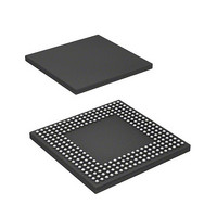
HD6417712BPV Renesas Electronics America, HD6417712BPV Datasheet - Page 484

HD6417712BPV
Manufacturer Part Number
HD6417712BPV
Description
MPU 1.5/3.3V 0K PB-FREE 256-BGA
Manufacturer
Renesas Electronics America
Series
SuperH® SH Ethernetr
Datasheet
1.HD6417712BPV.pdf
(980 pages)
Specifications of HD6417712BPV
Core Processor
SH-3 DSP
Core Size
32-Bit
Speed
200MHz
Connectivity
EBI/EMI, Ethernet, FIFO, SCI, SIO
Peripherals
DMA, POR, WDT
Number Of I /o
24
Program Memory Type
ROMless
Ram Size
16K x 8
Voltage - Supply (vcc/vdd)
1.4 V ~ 1.6 V
Oscillator Type
External
Operating Temperature
-20°C ~ 75°C
Package / Case
256-BGA
Lead Free Status / RoHS Status
Lead free / RoHS Compliant
Eeprom Size
-
Program Memory Size
-
Data Converters
-
Available stocks
Company
Part Number
Manufacturer
Quantity
Price
Company:
Part Number:
HD6417712BPV
Manufacturer:
Renesas Electronics America
Quantity:
10 000
- Current page: 484 of 980
- Download datasheet (6Mb)
Section 12 Bus State Controller (BSC)
12.5.6
The burst ROM (clock asynchronous) interface is used to access a memory with a high-speed read
function using a method of address switching called the burst mode or page mode. In a burst ROM
(clock asynchronous) interface, basically the same access as the normal space is performed, but
the 2nd and subsequent accesses are performed only by changing the address, without negating the
RD signal at the end of the 1st cycle. In the 2nd and subsequent accesses, addresses are changed at
the falling edge of the CKIO.
For the 1st access cycle, the number of wait cycles specified by the W[3:0] bits in CSnWCR is
inserted. For the 2nd and subsequent access cycles, the number of wait cycles specified by the
BW[1:0] bits in CSnWCR is inserted.
In the access to the burst ROM (clock asynchronous), the BS signal is asserted only to the first
access cycle. An external wait input is valid only to the first access cycle.
In the single access or write access that do not perform the burst operation in the burst ROM
(clock asynchronous) interface, access timing is same as a normal space.
Rev. 1.00 Dec. 27, 2005 Page 440 of 932
REJ09B0269-0100
Burst ROM (Clock Asynchronous) Interface
A12/A11*
A25 to A0
D31 to D0
DACKn*
DQMxx
RD/WR
CKIO
CKE
RAS
CAS
CSn
BS
Figure 12.31 Transition Timing in Deep Power-Down Mode
1
2
Notes: 1. Address pin to be connected to the A10 pin of SDRAM.
2. The waveform for DACKn is when active low is specified.
Tp
Tpw
Tdpd
Trc
Trc
Hi-Z
Trc
Trc
Trc
Related parts for HD6417712BPV
Image
Part Number
Description
Manufacturer
Datasheet
Request
R

Part Number:
Description:
KIT STARTER FOR M16C/29
Manufacturer:
Renesas Electronics America
Datasheet:

Part Number:
Description:
KIT STARTER FOR R8C/2D
Manufacturer:
Renesas Electronics America
Datasheet:

Part Number:
Description:
R0K33062P STARTER KIT
Manufacturer:
Renesas Electronics America
Datasheet:

Part Number:
Description:
KIT STARTER FOR R8C/23 E8A
Manufacturer:
Renesas Electronics America
Datasheet:

Part Number:
Description:
KIT STARTER FOR R8C/25
Manufacturer:
Renesas Electronics America
Datasheet:

Part Number:
Description:
KIT STARTER H8S2456 SHARPE DSPLY
Manufacturer:
Renesas Electronics America
Datasheet:

Part Number:
Description:
KIT STARTER FOR R8C38C
Manufacturer:
Renesas Electronics America
Datasheet:

Part Number:
Description:
KIT STARTER FOR R8C35C
Manufacturer:
Renesas Electronics America
Datasheet:

Part Number:
Description:
KIT STARTER FOR R8CL3AC+LCD APPS
Manufacturer:
Renesas Electronics America
Datasheet:

Part Number:
Description:
KIT STARTER FOR RX610
Manufacturer:
Renesas Electronics America
Datasheet:

Part Number:
Description:
KIT STARTER FOR R32C/118
Manufacturer:
Renesas Electronics America
Datasheet:

Part Number:
Description:
KIT DEV RSK-R8C/26-29
Manufacturer:
Renesas Electronics America
Datasheet:

Part Number:
Description:
KIT STARTER FOR SH7124
Manufacturer:
Renesas Electronics America
Datasheet:

Part Number:
Description:
KIT STARTER FOR H8SX/1622
Manufacturer:
Renesas Electronics America
Datasheet:

Part Number:
Description:
KIT DEV FOR SH7203
Manufacturer:
Renesas Electronics America
Datasheet:


