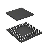
HD6417712BPV Renesas Electronics America, HD6417712BPV Datasheet - Page 502

HD6417712BPV
Manufacturer Part Number
HD6417712BPV
Description
MPU 1.5/3.3V 0K PB-FREE 256-BGA
Manufacturer
Renesas Electronics America
Series
SuperH® SH Ethernetr
Datasheet
1.HD6417712BPV.pdf
(980 pages)
Specifications of HD6417712BPV
Core Processor
SH-3 DSP
Core Size
32-Bit
Speed
200MHz
Connectivity
EBI/EMI, Ethernet, FIFO, SCI, SIO
Peripherals
DMA, POR, WDT
Number Of I /o
24
Program Memory Type
ROMless
Ram Size
16K x 8
Voltage - Supply (vcc/vdd)
1.4 V ~ 1.6 V
Oscillator Type
External
Operating Temperature
-20°C ~ 75°C
Package / Case
256-BGA
Lead Free Status / RoHS Status
Lead free / RoHS Compliant
Eeprom Size
-
Program Memory Size
-
Data Converters
-
Available stocks
Company
Part Number
Manufacturer
Quantity
Price
Company:
Part Number:
HD6417712BPV
Manufacturer:
Renesas Electronics America
Quantity:
10 000
- Current page: 502 of 980
- Download datasheet (6Mb)
Section 12 Bus State Controller (BSC)
In write-through mode, the cache is first searched. If data is detected at the address corresponding
to the cache, the data is re-written to the cache simultaneously with the actual write via the internal
bus. If data is not detected at the address corresponding to the cache, the cache is not modified but
an actual write is performed via the internal bus.
Since the bus state controller (BSC) incorporates a one-stage write buffer, the BSC can execute an
access via the internal bus before the previous external bus cycle is completed in a write cycle. If
the on-chip module is read or written after the external low-speed memory is written, the on-chip
module can be accessed before the completion of the external low-speed memory write cycle.
In read cycles, the CPU is placed in the wait state until read operation has been completed. To
continue the process after the data write to the device has been completed, perform a dummy read
to the same address to check for completion of the write before the next process to be executed.
The write buffer of the BSC functions in the same way for an access by a bus master other than
the CPU such as the DMAC or E-DMAC. Accordingly, to perform dual address DMA transfers,
the next read cycle is initiated before the previous write cycle is completed. Note, however, that if
both the DMA source and destination addresses exist in external memory space, the next write
cycle will not be initiated until the previous write cycle is completed.
On-Chip Peripheral Module Access: To access an on-chip module register, two or more
peripheral module clock (Pφ) cycles are required. Care must be taken in system design.
Rev. 1.00 Dec. 27, 2005 Page 458 of 932
REJ09B0269-0100
Related parts for HD6417712BPV
Image
Part Number
Description
Manufacturer
Datasheet
Request
R

Part Number:
Description:
KIT STARTER FOR M16C/29
Manufacturer:
Renesas Electronics America
Datasheet:

Part Number:
Description:
KIT STARTER FOR R8C/2D
Manufacturer:
Renesas Electronics America
Datasheet:

Part Number:
Description:
R0K33062P STARTER KIT
Manufacturer:
Renesas Electronics America
Datasheet:

Part Number:
Description:
KIT STARTER FOR R8C/23 E8A
Manufacturer:
Renesas Electronics America
Datasheet:

Part Number:
Description:
KIT STARTER FOR R8C/25
Manufacturer:
Renesas Electronics America
Datasheet:

Part Number:
Description:
KIT STARTER H8S2456 SHARPE DSPLY
Manufacturer:
Renesas Electronics America
Datasheet:

Part Number:
Description:
KIT STARTER FOR R8C38C
Manufacturer:
Renesas Electronics America
Datasheet:

Part Number:
Description:
KIT STARTER FOR R8C35C
Manufacturer:
Renesas Electronics America
Datasheet:

Part Number:
Description:
KIT STARTER FOR R8CL3AC+LCD APPS
Manufacturer:
Renesas Electronics America
Datasheet:

Part Number:
Description:
KIT STARTER FOR RX610
Manufacturer:
Renesas Electronics America
Datasheet:

Part Number:
Description:
KIT STARTER FOR R32C/118
Manufacturer:
Renesas Electronics America
Datasheet:

Part Number:
Description:
KIT DEV RSK-R8C/26-29
Manufacturer:
Renesas Electronics America
Datasheet:

Part Number:
Description:
KIT STARTER FOR SH7124
Manufacturer:
Renesas Electronics America
Datasheet:

Part Number:
Description:
KIT STARTER FOR H8SX/1622
Manufacturer:
Renesas Electronics America
Datasheet:

Part Number:
Description:
KIT DEV FOR SH7203
Manufacturer:
Renesas Electronics America
Datasheet:


