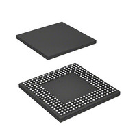
HD6417712BPV Renesas Electronics America, HD6417712BPV Datasheet - Page 758

HD6417712BPV
Manufacturer Part Number
HD6417712BPV
Description
MPU 1.5/3.3V 0K PB-FREE 256-BGA
Manufacturer
Renesas Electronics America
Series
SuperH® SH Ethernetr
Datasheet
1.HD6417712BPV.pdf
(980 pages)
Specifications of HD6417712BPV
Core Processor
SH-3 DSP
Core Size
32-Bit
Speed
200MHz
Connectivity
EBI/EMI, Ethernet, FIFO, SCI, SIO
Peripherals
DMA, POR, WDT
Number Of I /o
24
Program Memory Type
ROMless
Ram Size
16K x 8
Voltage - Supply (vcc/vdd)
1.4 V ~ 1.6 V
Oscillator Type
External
Operating Temperature
-20°C ~ 75°C
Package / Case
256-BGA
Lead Free Status / RoHS Status
Lead free / RoHS Compliant
Eeprom Size
-
Program Memory Size
-
Data Converters
-
Available stocks
Company
Part Number
Manufacturer
Quantity
Price
Company:
Part Number:
HD6417712BPV
Manufacturer:
Renesas Electronics America
Quantity:
10 000
- Current page: 758 of 980
- Download datasheet (6Mb)
Section 18 Ethernet Controller (EtherC)
shows the connection example of the external CAM logic while figure 18.6 shows the timing
conditions of the external CAM signal.
The setting on whether to enable or disable the referencing of external CAM logic evaluation
results by the CAMSEN0 and CAMSEN1 pins is carried out by the transfer function setting
register (common) (TSU_FWSLC). When referencing of the CAMSEN0 and CAMSEN1 pins is
enabled during receive, it is determined whether to send or discard the frames input from to MAC-
0/1 to E-DMAC0/1 (have E-DMAC receive the frames) according to the value of the CAMSEN0
or CAMSEN1 pin. When relaying and CAMSEN0/1 pin referencing are enabled at the same time,
the transfer or discard of multicast frames and frames to destinations other than this LSI can be
determined by the value of the CAMSEN0 and CAMSEN1 pins.
Table 18.5 shows the processing method (receive or discard) for frames in MAC0 to E-DMAC0 or
MAC1 to E-DMAC1 reception, while Table 18.6 shows the processing method (receive or
discard) for frames in MAC0 to MAC1 or MAC1 to MAC relay. The external CAM logic is
memorized with MAC addresses different from the CAM entry table in this LSI. When the MAC
address received from the PHY matches the destination address memorized in the external CAM
logic, the CAMSEN0 or CAMSEN1 pin is asserted*. EtherC receives or discards the frames when
CAMSEN0/1 was asserted according to the settings in table 18.5.
Figure 18.6 shows the valid range of CAMSEN0/1 assertion for the corresponding receive frames.
Rev. 1.00 Dec. 27, 2005 Page 714 of 932
REJ09B0269-0100
External memory
Descriptor
Figure 18.5 Example of External CAM Connection
This LSI
EtherC
CAM logic
External
CAMSEN0 or
CAMSEN1 pin
MII (RX-DV, RXD3 to RXD0)
PHY-LSI
Related parts for HD6417712BPV
Image
Part Number
Description
Manufacturer
Datasheet
Request
R

Part Number:
Description:
KIT STARTER FOR M16C/29
Manufacturer:
Renesas Electronics America
Datasheet:

Part Number:
Description:
KIT STARTER FOR R8C/2D
Manufacturer:
Renesas Electronics America
Datasheet:

Part Number:
Description:
R0K33062P STARTER KIT
Manufacturer:
Renesas Electronics America
Datasheet:

Part Number:
Description:
KIT STARTER FOR R8C/23 E8A
Manufacturer:
Renesas Electronics America
Datasheet:

Part Number:
Description:
KIT STARTER FOR R8C/25
Manufacturer:
Renesas Electronics America
Datasheet:

Part Number:
Description:
KIT STARTER H8S2456 SHARPE DSPLY
Manufacturer:
Renesas Electronics America
Datasheet:

Part Number:
Description:
KIT STARTER FOR R8C38C
Manufacturer:
Renesas Electronics America
Datasheet:

Part Number:
Description:
KIT STARTER FOR R8C35C
Manufacturer:
Renesas Electronics America
Datasheet:

Part Number:
Description:
KIT STARTER FOR R8CL3AC+LCD APPS
Manufacturer:
Renesas Electronics America
Datasheet:

Part Number:
Description:
KIT STARTER FOR RX610
Manufacturer:
Renesas Electronics America
Datasheet:

Part Number:
Description:
KIT STARTER FOR R32C/118
Manufacturer:
Renesas Electronics America
Datasheet:

Part Number:
Description:
KIT DEV RSK-R8C/26-29
Manufacturer:
Renesas Electronics America
Datasheet:

Part Number:
Description:
KIT STARTER FOR SH7124
Manufacturer:
Renesas Electronics America
Datasheet:

Part Number:
Description:
KIT STARTER FOR H8SX/1622
Manufacturer:
Renesas Electronics America
Datasheet:

Part Number:
Description:
KIT DEV FOR SH7203
Manufacturer:
Renesas Electronics America
Datasheet:


